Semiconductor laser diode device and manufacturing method thereof

a laser diode and semiconductor technology, applied in semiconductor lasers, laser details, electrical devices, etc., can solve the problems of increased resistance and voltage of the device, increased cod, and difficult to use the two etching methods, etc., to improve the contact resistance, the beam shape, and the driving voltage.

Pending Publication Date: 2022-04-21
QSI
View PDF0 Cites 0 Cited by
  • Summary
  • Abstract
  • Description
  • Claims
  • Application Information

AI Technical Summary

Benefits of technology

[0029]According to the present disclosure, the regrowth process of the second upper clad (P clad) is applied to control appropriately the area of the wave guide, thereby impro

Problems solved by technology

For example, when the wave guide is wide, a problem such as a multi-mode, a kink or a catastrophic optical damage (COD) may occur, and when the wavelength is too small, an internal resistance Rd or a voltage V is increased to generate the heat of the device.
In the high-power and high-reliability laser diode with the thick second upper clad (P clad), it is difficult to use the two etching methods.
As a result, if the size of a lower portion Wb of the wave guide is adjusted, an upper portion Wt of the wave guide is narrowed, the resistance and the voltage of the device are increased, and thus, there is a problem that the power and the reliability are deteriorated.
Second, in the case of dry etching, the sizes of the upper and lower portions of the wave guide may be accurately controlled, but since a sheet of wafer is

Method used


Image

  • Semiconductor laser diode device and manufacturing method thereof
  • Semiconductor laser diode device and manufacturing method thereof
  • Semiconductor laser diode device and manufacturing method thereof

Examples


Embodiment Construction

[0041]Hereinafter, a preferred embodiment of the present disclosure will be described in detail with reference to the accompanying drawings.

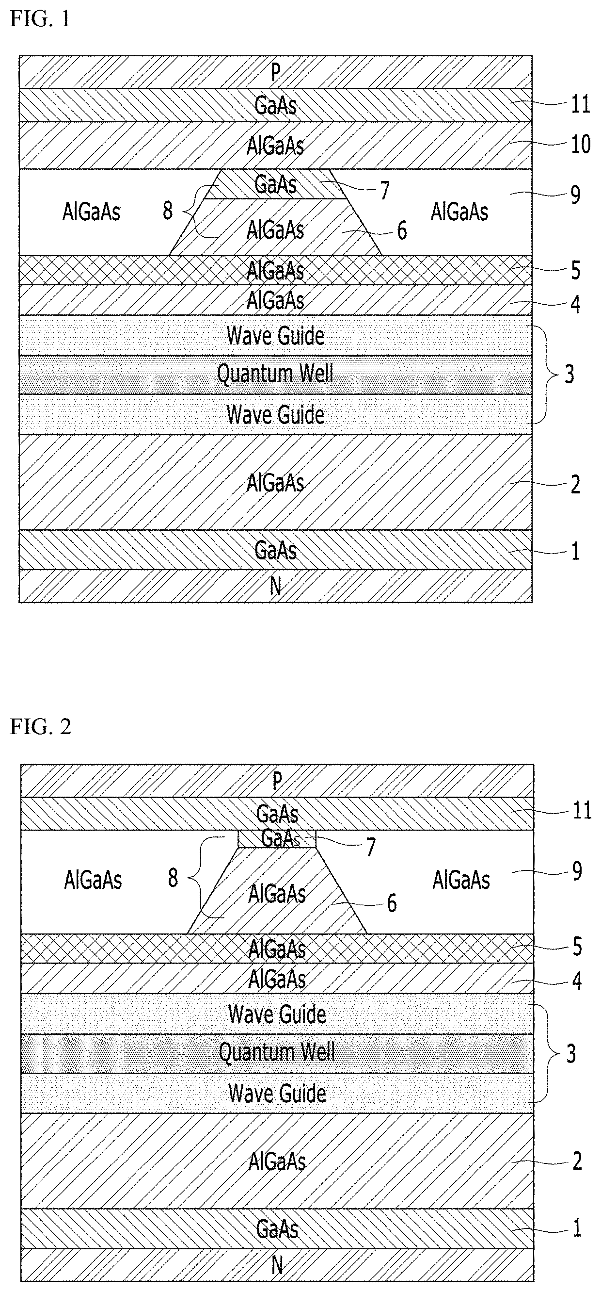
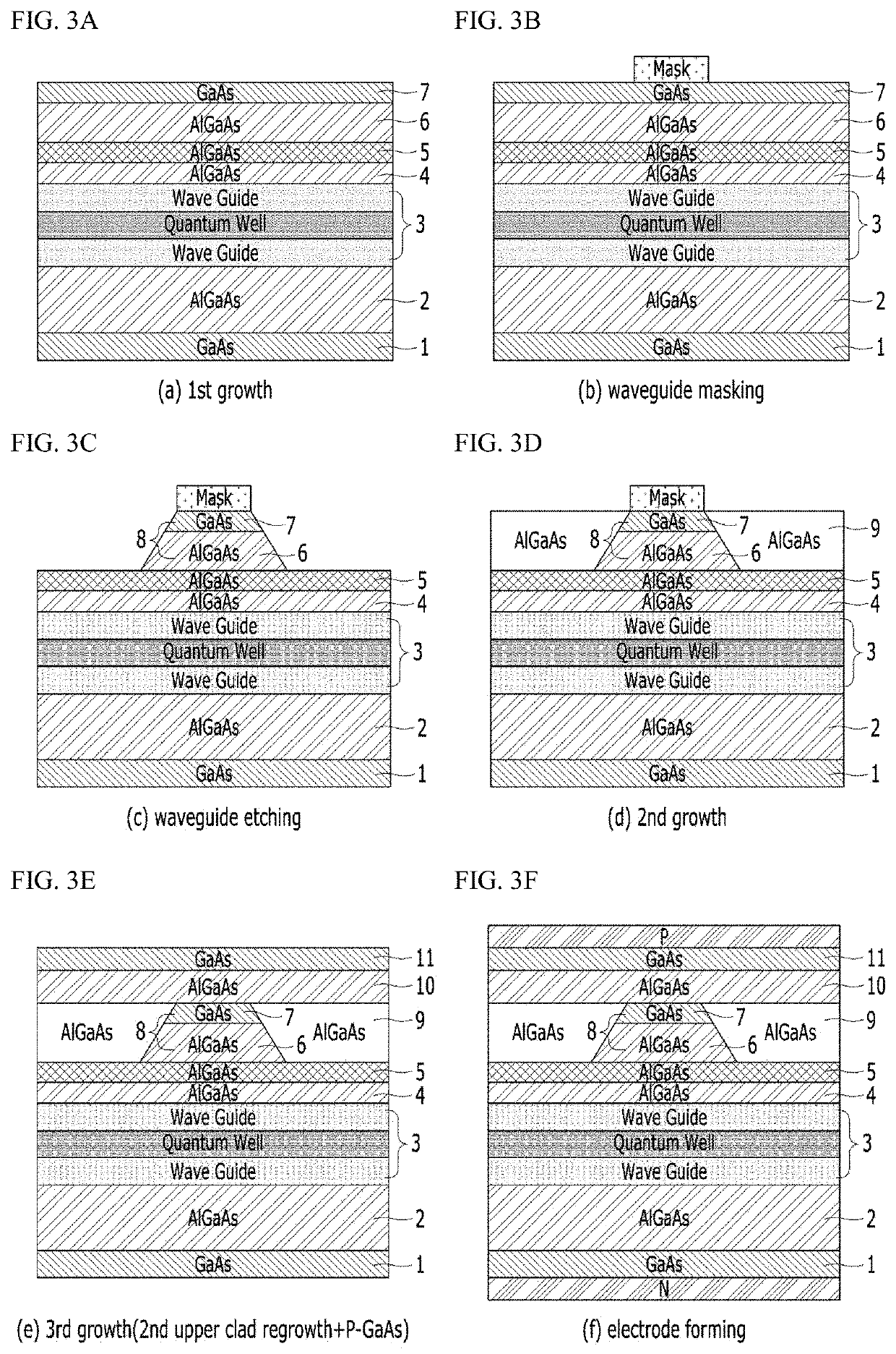
[0042]FIG. 1 is a cross-sectional view of a schematic diagram of improving a high-power and high-reliability device of which a second upper clad is thick through the second upper clad (P clad) regrowth according to an embodiment of the present disclosure. The high-power and high-reliability device consists of a lower clad layer 2, an active layer 3, a first upper clad layer 4, an etch stop layer 5, a second upper clad layer 6, and an anti-oxidation layer 7 on a compound semiconductor substrate 1 in sequence.

[0043]When describing a material and a growth order of primary growth of the high-power and high-reliability laser diode in detail, the substrate 1 consists of an n-type GaAs compound semiconductor. In this case, the lower clad layer 2 consists of n-type AlxGaAs (Alx composition is 0.5 to 0.6) and the doping of the lower clad layer 2 is perfo...


PUM


Abstract

The present disclosure provides fabrication of a laser diode with reliability at a high temperature of 80° C. or more in a high-power single mode by a process of thinly growing a second upper clad (P clad) layer at 1 μm or less in primary growth, appropriately controlling an upper portion Wt to 1.5 μm or more and a lower portion Wb to 4.0 μm or less of the wave guide, and then compensating for a second upper clad layer to 0.5 μm or more in regrowth, in order to compensate for disadvantages of a high-power and high-reliability laser diode device with a thick second upper clad layer (P clad). A second upper clad regrowth layer is applied to reduce internal resistance and voltage and reduce heat generated in the device to increase a Kink and a COD power, thereby improving the performance of a high-power and high-reliability laser diode.

Description

CROSS-REFERENCE TO RELATED APPLICATIONS[0001]This application claims the priority of Korean Patent Application No. 10-2020-0134106 filed on Oct. 16, 2020, in the Korean Intellectual Property Office, the disclosure of which is incorporated herein by reference.BACKGROUND OF THE INVENTIONField of the Invention[0002]The present disclosure relates to a semiconductor laser diode device and a manufacturing method thereof used for optical devices such as a dust measurement sensor, a factory automation sensor, an optical recording medium, and a laser printer.Description of the Related Art[0003]In recent years, at home and abroad, as interests in (micro) fine dust generation and environment are increased, diversification of particle-related application products is made. Particularly, as microfine dust with a size of PM 2.5 or less occurs at about 90% of the total share, a laser diode has been used as a lighting source of the dust sensor. The laser diode is used as a light source for detecting...

Claims


Application Information

Patent Timeline
IPC IPC(8): H01S5/227H01S5/343
CPCH01S5/2275H01S2304/04H01S5/3432H01S5/34353H01S5/0021H01S5/0014H01S5/2231H01S5/3213H01S5/323H01S5/04252H01S5/227H01S5/18344H01S5/309
Inventor KWAK, JEONG-GEUNCHOI, AN SIKKIM, TAEKYUNG
Owner QSI
Why Eureka
Try Eureka