Flash memory cell and method for manufacturing the same

Inactive Publication Date: 2005-06-30
DONGBU ELECTRONICS CO LTD +1
View PDF2 Cites 0 Cited by
  • Summary
  • Abstract
  • Description
  • Claims
  • Application Information

AI Technical Summary

Benefits of technology

[0012] The present invention has been made in an effort to solve the above problems, and an object of the present is t

Problems solved by technology

However, metal contacts from adjoining flash memory cells to an overlying metal common source line may not be appropriate for a large scale integrated circuit in consideration of the contact margin and cell real estate consumed by the metal source line.
However, the conventional SAS technique depicted in FIG. 2 has a drawback in that the contact resistance of the common

Method used


Image

  • Flash memory cell and method for manufacturing the same
  • Flash memory cell and method for manufacturing the same
  • Flash memory cell and method for manufacturing the same

Examples


Example

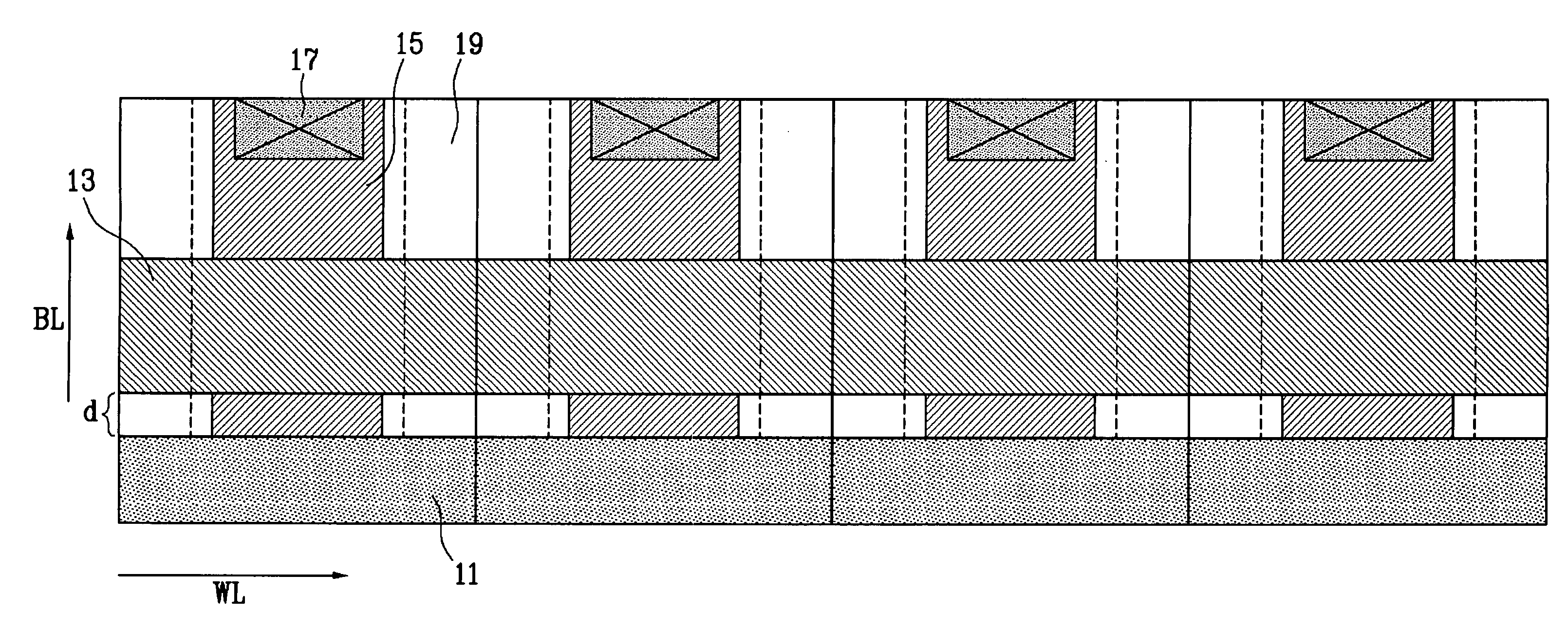
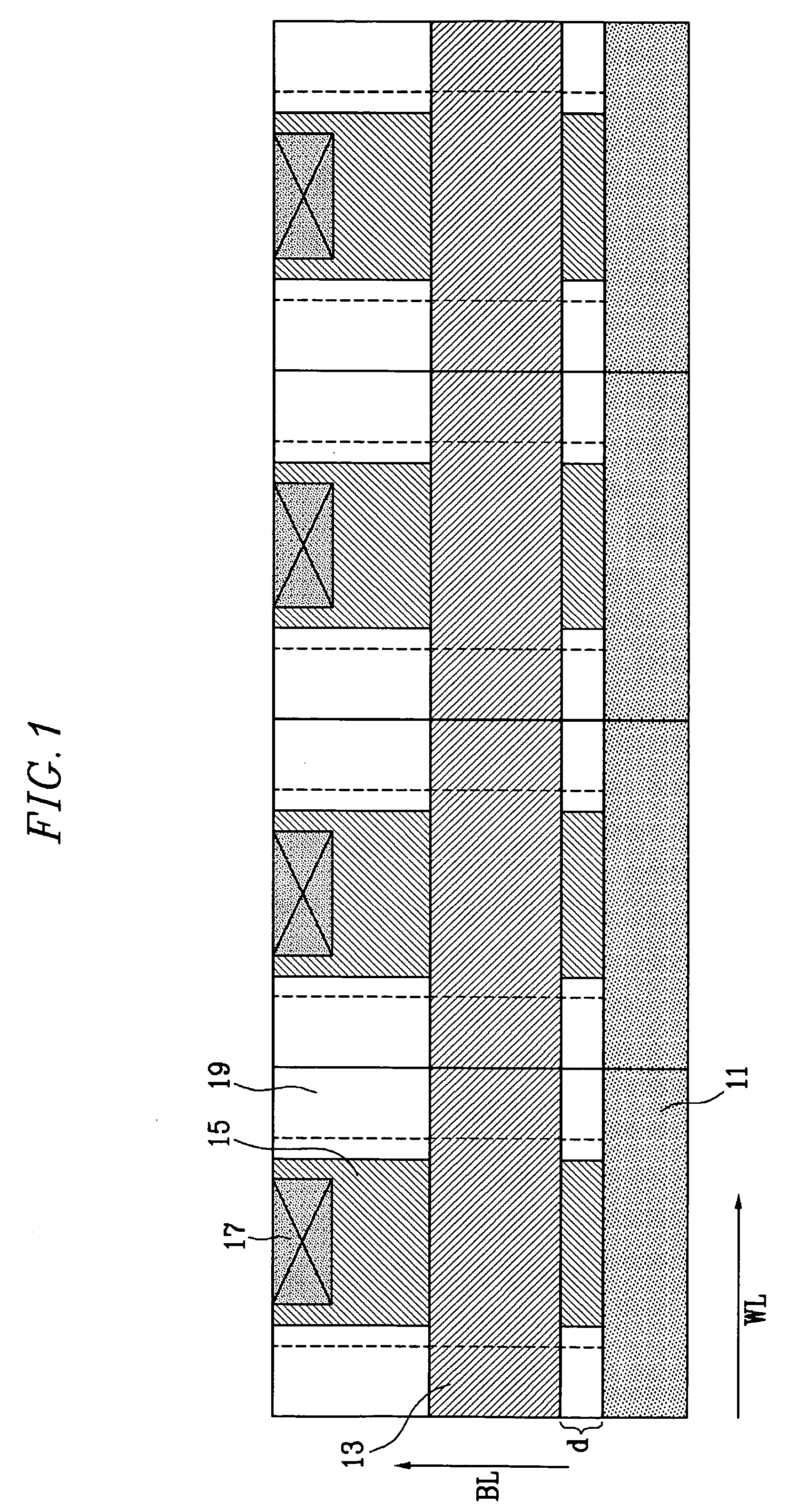
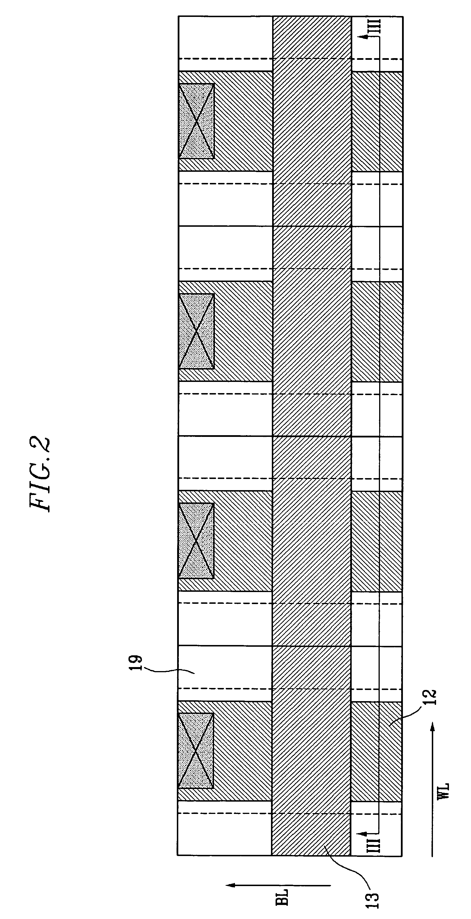
[0026] Preferred embodiments of the present invention will be described in detail hereinafter with reference to the accompanying drawings.

[0027]FIG. 3 is a cross-sectional view illustrating a memory cell structure manufactured according to a conventional SAS technique, which is cut along the line III-III of FIG. 2. As shown in FIG. 3, the memory cell manufactured according to the conventional method adopting the SAS technique is provided with a trench 19 corresponding to a device isolation region and a common source line 12 formed by ion injecting impurities in a region for forming the common source line in a word line (WL) direction on the substrate 100. Since the above-structured common source line 12 is formed according to the profile of the trench 19 of the trench line, there is a shortcoming in that the contact resistance of the common source line per cell abruptly increases. In fact, the deeper the trench 19, or the steeper the slope of trench sidewall 190, the worse the volt...


PUM


Abstract

The present invention relates to a flash memory and a method for manufacturing the same, capable of minimizing resistance of the common source line in the flash memory cell manufacturing process. In the memory cell manufacturing method according to the embodiment of the present invention, trench lines are continuously formed on a semiconductor substrate, and gate oxide film lines are formed on the semiconductor substrate except at the trench lines. Sequentially, gate lines vertical with the trench lines are formed on the trench lines and the gate oxide film lines, and the dielectric material of the trench line and the gate dielectric film between adjacent gate lines is removed, and a conductive film of Ti/TiN or Co/Ti/TiN is deposited on the common source region, and then a silicide is formed on the common source region by means of annealing.

Description

BACKGROUND OF THE INVENTION [0001] (a) Field of the Invention [0002] The present invention relates to a flash memory cell and a method for manufacturing the same, and in particular, to the flash memory cell and a method for manufacturing the same that are capable of minimizing resistance of the common source line in a fabrication process for an Embedded Flash Memory Cell. [0003] (b) Description of the Related Art [0004] Typically, a flash memory device is manufactured so as to secure the advantages of the EPROM having programmable and erasable characteristics, and the EEPROM having electrically programmable and erasable characteristics. Such a flash memory includes a thin tunnel oxide formed on a silicon substrate, a floating gate and a control gate deposited with an interposed dielectric film, and a source / drain region formed on an exposed area of the substrate, the device storing 1 bit at one transistor and being electrically programmable and erasable. [0005] Such a flash memory d...

Claims


Application Information

Patent Timeline
IPC IPC(8): H01L21/336H01L21/8247H01L27/115
CPCH01L27/115H01L27/11521H01L27/11519H10B41/10H10B69/00H10B41/30
Inventor JUNG, MYUNG-JIN
Owner DONGBU ELECTRONICS CO LTD
Why Eureka
Try Eureka