
Light scattering element, optical scanning device, and image displaying device

Active Publication Date: 2012-08-30
STANLEY ELECTRIC CO LTD
View PDF3 Cites 14 Cited by
  • Summary
  • Abstract
  • Description
  • Claims
  • Application Information

AI Technical Summary

Benefits of technology

[0010]The present invention is made in view of above background and aims to provide a light scattering element capable of decreasing the speckle noise of laser light, by forming the element itself to be capable of vibrating. Further, the present invention aims to provide an optical scanning device and an image projecting device capable of reducing the speckle noise of laser light, by using the light scattering element, without providing additional lens or driving mechanism such as a vibrating means, which is compact and has simple structure.

Problems solved by technology

However, in the case where the laser light source is used as the light source, there arises a problem that speckle noise (granular interference pattern) is generated and the image quality becomes degraded.
That is, the speckle noise is superimposed on the image which significantly degrades the image quality.
As such, in the techniques such as those disclosed in Japanese Patent Laid-Open No. 2002-62582 and Japanese Patent Laid-Open No. 2004-138669, various problems arose such as increase in the number of components, increase in the size as the system, increase in power consumption, and burden of optical alignment.

Method used


Image

  • Light scattering element, optical scanning device, and image displaying device
  • Light scattering element, optical scanning device, and image displaying device
  • Light scattering element, optical scanning device, and image displaying device

Examples


first embodiment

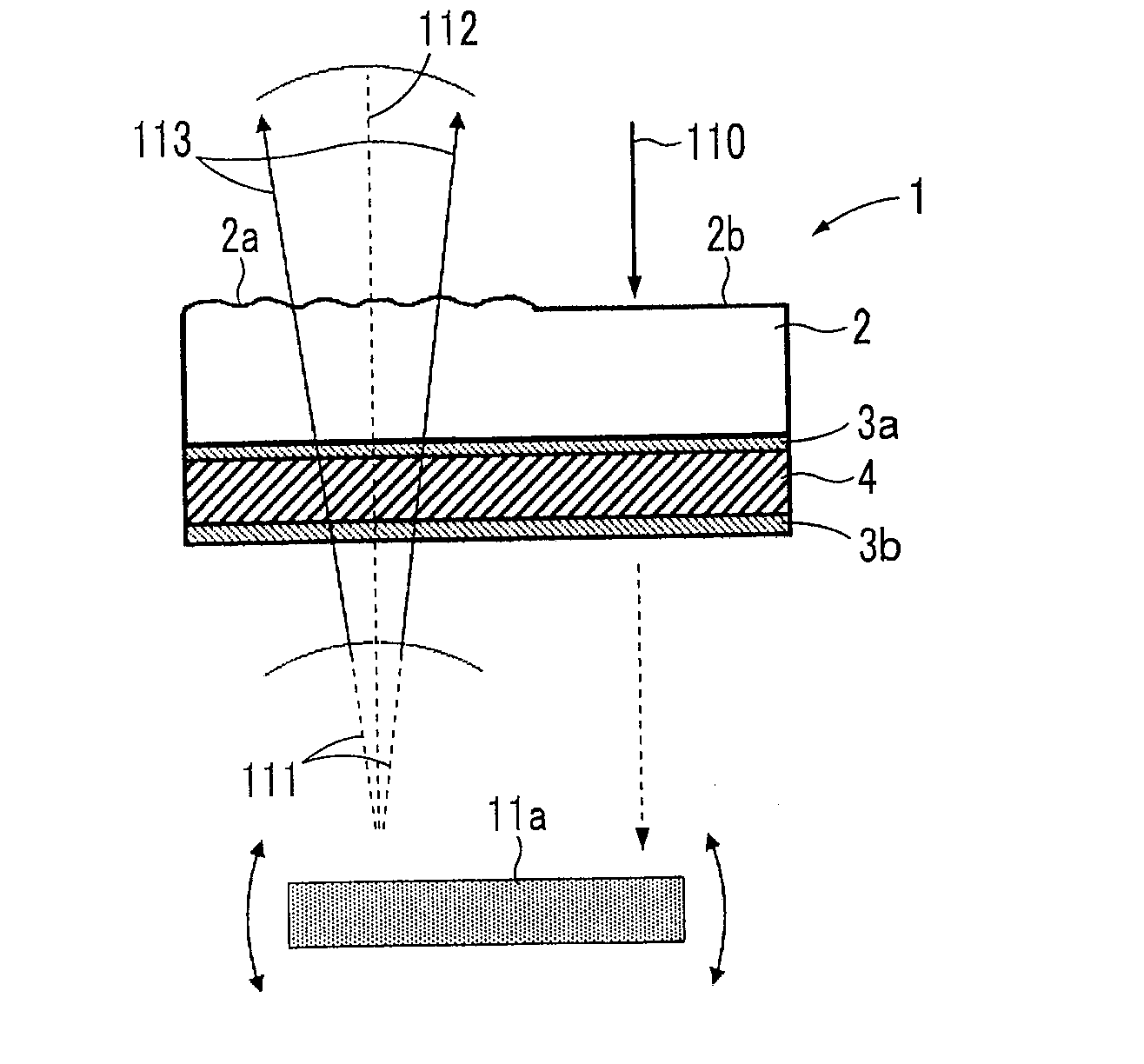
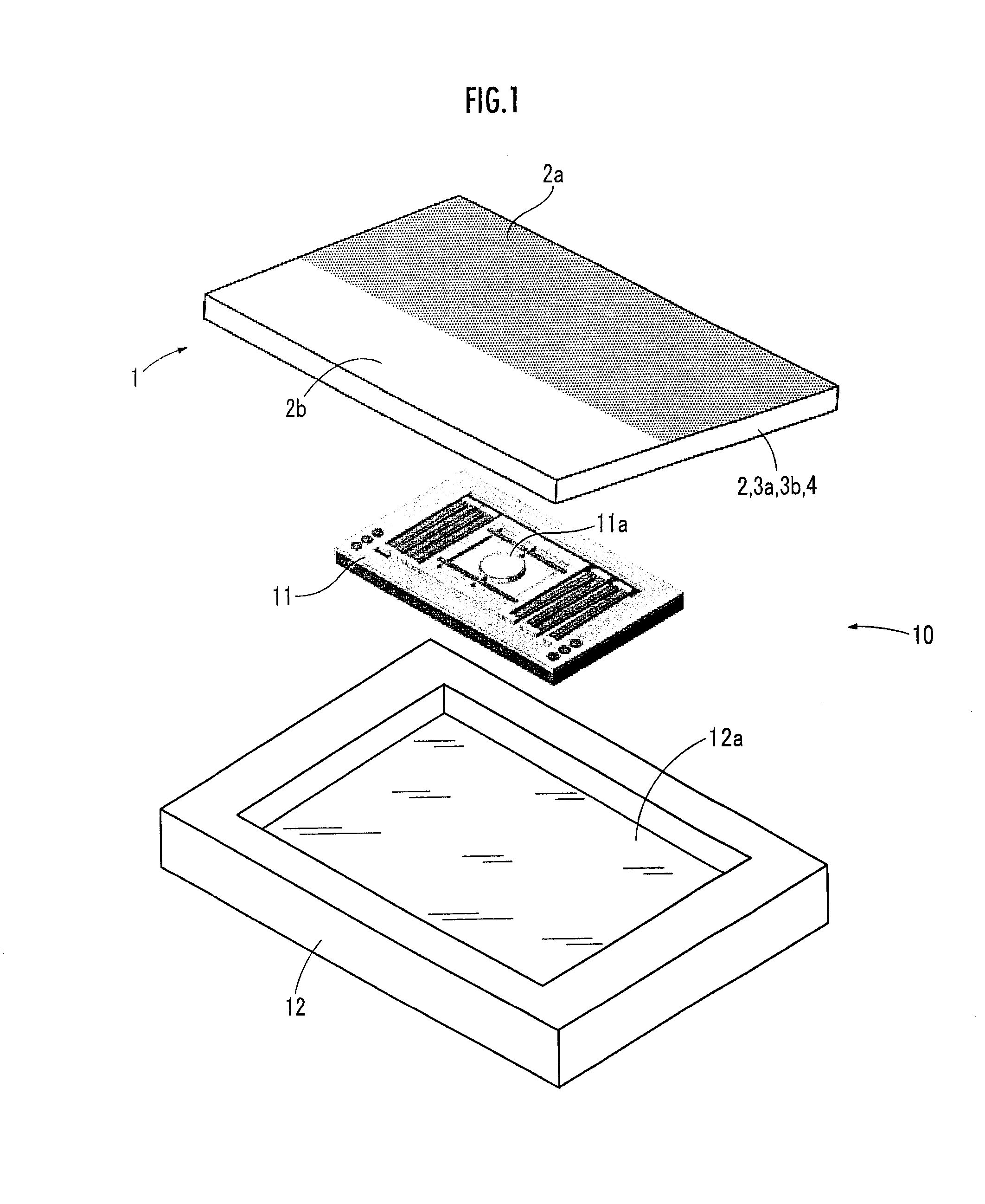
[0029]With reference to FIG. 1 through FIG. 4, explanation will be given on a light deflector using a light scattering element of a first embodiment of the present invention, for two-dimensionally scanning laser light and forming image on a screen. In the first embodiment, a light scattering element 1 is used as an optical window of a light deflector 10.

[0030]The light scattering element 1 is equipped with an optical element 2 which is transparent and is formed into a thin film, two electrodes 3a, 3b that are transparent and are formed into thin films, and a piezoelectric element 4 which is transparent and is formed into a thin film using lead zirconium titanate (PZT).

[0031]The optical element 2 is formed from a transparent resin (for example, acryl or polycarbonate) or a glass sheet which is treated at the surface with an optical scattering surface 2a by injection molding or imprint treating. When the transparent resin sheet is used for the optical element 2, the light scattering e...

second embodiment

[0066]Next, with reference to FIG. 5 and FIG. 6, explanation will be given on an image projecting device for forming image on a screen by a laser light using a light scattering element of a second embodiment of the present invention. In the second embodiment, a light scattering element 6 is used as the optical window of an image projecting device 30.

[0067]The image projecting device 30 is equipped with a laser light source 31, a light deflector 32, a control circuit 33, and the light scattering element 6.

[0068]The laser light source 31 is a light source which emits laser light to the light deflector 32. The light deflector 32 deflects the laser light from the laser light source 31 by an oscillation mirror (not shown) included therein, and emits the same to outside the image projecting device 30. The control circuit 33 controls the operation of the laser light source 31 and the light deflector 32. The light deflector 32 of the second embodiment is different from the light deflector 1...


PUM


Abstract

A light scattering element 1 is equipped with a transparent, thin film-like optical element 2 which scatters incident laser light, and a thin film-like piezoelectric element 4, which is sandwiched between two electrodes 3a, 3b and which is laminated on a surface of the optical element 2 that is different from an optical scattering surface 2a. The light scattering element 1 averages a speckle pattern of laser light scatted by the optical scattering surface 2a and emitted therefrom by vibration of the piezoelectric element 4 generated when alternating voltage is applied between the two electrodes 3a, 3b.

Description

BACKGROUND OF THE INVENTION[0001]1. Field of the Invention[0002]The present invention relates to a light scattering element, an optical scanning device, and an image displaying device which reduces speckle noise of laser light.[0003]2. Description of the Related Art[0004]Conventionally, there has been proposed, as one embodiment of an image display device, a projection display which displays an image on a screen, by projecting light from a light source to the screen while deflecting the same with a light deflector. As the light deflector, for example, a light deflector which integrally forms mechanical components such as a mirror and a piezoelectric actuator on a semiconductor substrate, has been proposed. This light deflector is one type of MEMS (micro electro mechanical systems) device using semiconductor process or micromachine technology (for example, refer to Japanese Patent Laid-Open No. 2005-148459). In this light deflector, one end of the piezoelectric actuator is coupled to...

Claims


Application Information

Patent Timeline
IPC IPC(8): G02B26/10
CPCG02B5/0215G02B27/48G02B26/105G02B26/00
Inventor YASUDA, YOSHIAKI
Owner STANLEY ELECTRIC CO LTD
Features
  • Generate Ideas
  • Intellectual Property
  • Life Sciences
  • Materials
  • Tech Scout
  • Unparalleled Data Quality
  • Higher Quality Content
  • 60% Fewer Hallucinations
Learn More