Printed circuit board design for high speed application

Active Publication Date: 2012-09-13
MEDIATEK INC
View PDF14 Cites 19 Cited by
  • Summary
  • Abstract
  • Description
  • Claims
  • Application Information

AI Technical Summary

Problems solved by technology

Notwithstanding, along with rapid advances in printed circuit board technology, electromagnetic interference (EMI) problems have increased in severity.
When electronic devices/components operate in high speed and are allocated in the PCB with a high device density, noise may be generated and affect the operation of other electronic devices.
Crosstalk is a kind of noise induced primarily by the electromagnetic coupling between signal lines and degrades signal quality.
As more and more functions are integrated on a chip, more circuit traces of the printed circuit board are demanded, and thus the

Method used


Image

  • Printed circuit board design for high speed application
  • Printed circuit board design for high speed application
  • Printed circuit board design for high speed application

Examples


Embodiment Construction

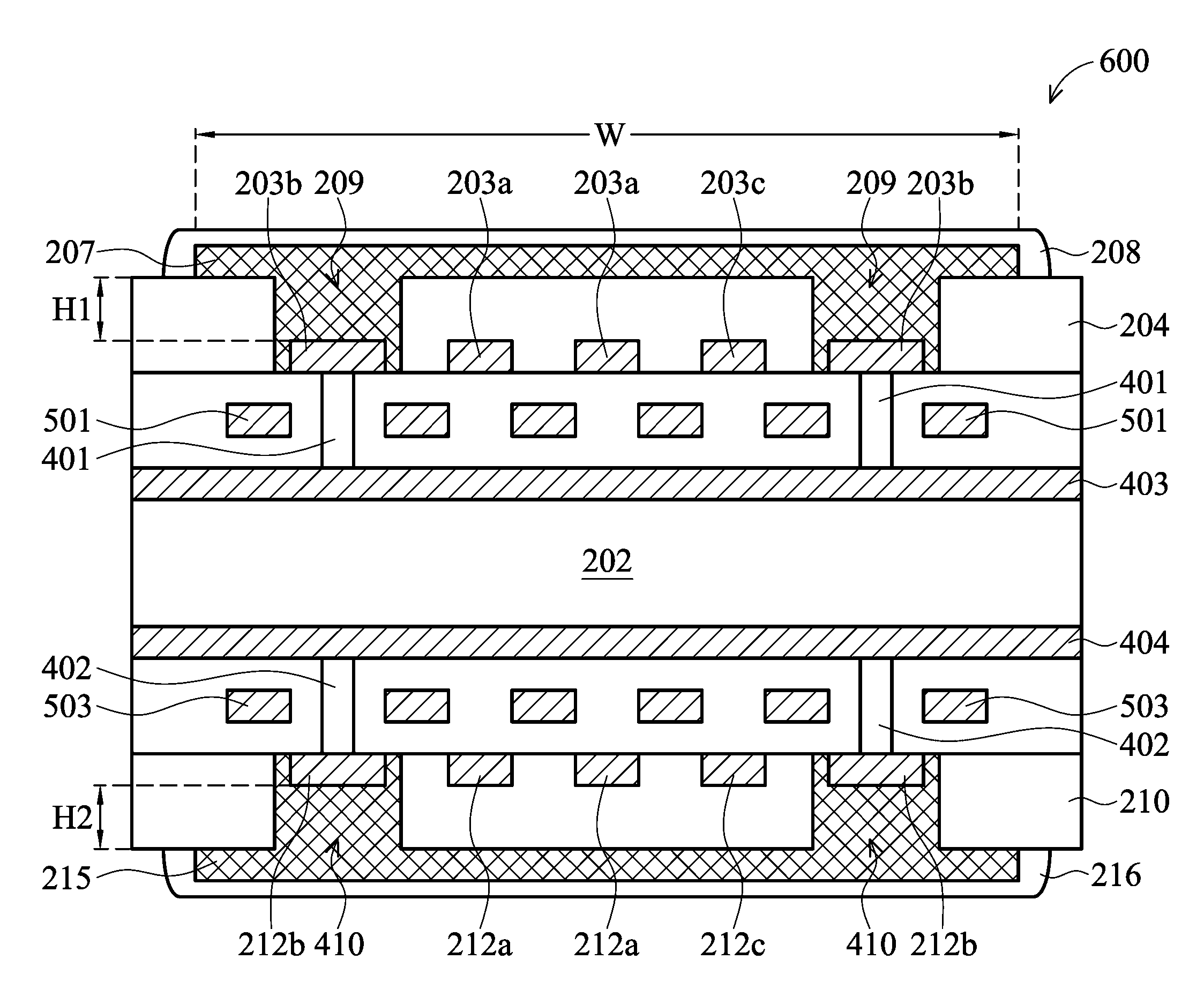
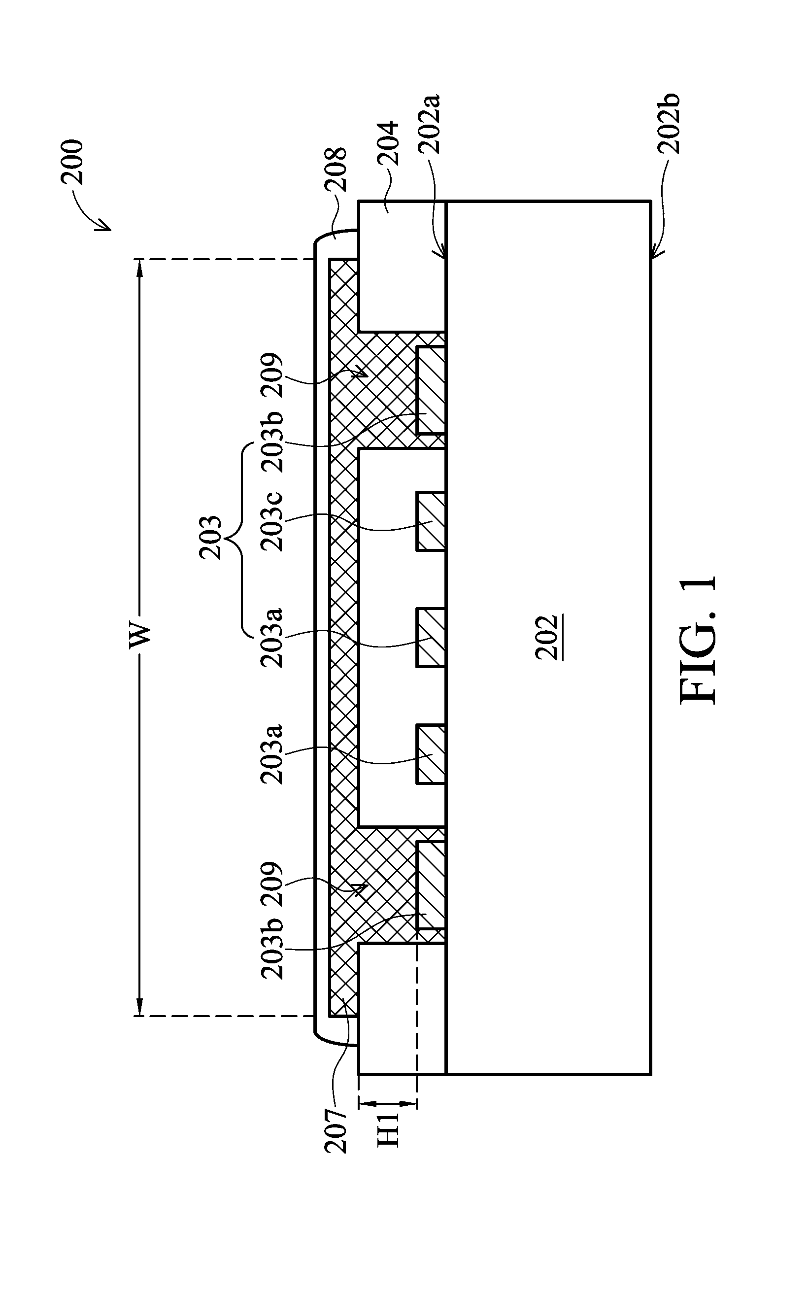
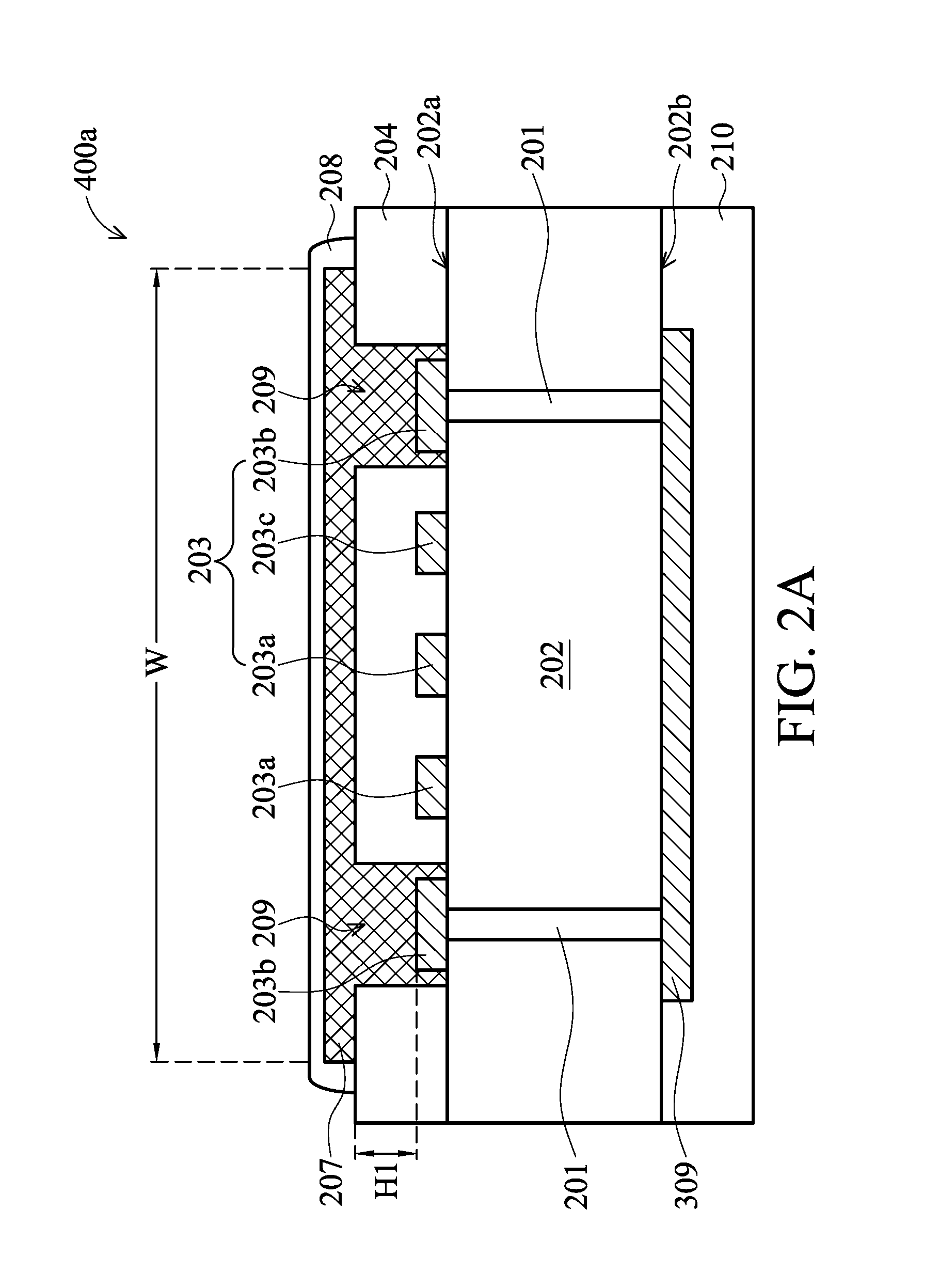
[0022]The following description encompasses the fabrication and the purpose of the invention. It can be understood that this description is provided for the purpose of illustrating the fabrication and the use of the invention and should not be taken in a limited sense. In the drawings or disclosure, the same or similar elements are represented or labeled by the same or similar symbols. Moreover, the shapes or thicknesses of the elements shown in the drawings may be magnified for simplicity and convenience. Additionally, the elements not shown or described in the drawings or disclosure are common elements which are well known in the art.

[0023]In the following various exemplary embodiments, the printed circuit board may comprise net, traces, strip lines, or micro-strip which are made of conductive material to electrically connect various electronic components for transmitting data and / or signals in a high speed manner. Such net, traces, strip lines, or micro-strip may be function as a...


PUM


Abstract

A printed circuit board (PCB) is disclosed. The PCB includes a substrate have a top surface and a bottom surface. A first conductive layer is disposed on the top surface of the substrate. The first conductive layer comprises a first signal net and a second signal net. An outermost insulating layer is disposed on the top surface of the substrate to cover the substrate and the first conductive layer. The outmost insulating layer comprises an opening to expose a portion of the second signal net. And, a second conductive layer is disposed on the outermost insulating layer and substantially covering at least a portion of the first signal net. The second conductive layer is filled into the opening to electrically connect to the second signal net which is able to provide one of a ground potential and a power potential.

Description

CROSS REFERENCE TO RELATED APPLICATIONS[0001]This application claims the benefit of U.S. Provisional Application No. 61 / 451,283, filed Mar. 10, 2011, the entirety of which is incorporated by reference herein.BACKGROUND OF THE INVENTION[0002]1. Field of the Invention[0003]The invention relates to a printed circuit board and more particularly to a printed circuit board design with good signal quality.[0004]2. Description of the Related Art[0005]Typically, a printed circuit board (PCB) is a layered insulating structure with internal and external traces / planes that allows electronic devices / components on the printed circuit board to be electrically connected to each other and to the outside environment. Printed circuit boards are the most commonly used packaging medium for electronic circuits. Due to the demand for high performance systems, packaging density and propagation speeds have increased, to force the technological development of the printed circuit boards to evolve from being s...

Claims


Application Information

Patent Timeline
IPC IPC(8): H05K1/02
CPCH05K2201/0715H01P3/08H05K1/0219H05K2201/09236H05K1/0224H05K1/0298
Inventor CHEN, NAN-JANG
Owner MEDIATEK INC
Why Eureka
Try Eureka