Substrates with through vias with conductive features for connection to integrated circuit elements, and methods for forming through vias in substrates

a technology of integrated circuit elements and substrates, which is applied in the direction of printed circuit aspects, printed circuit electric connection formation, printed circuit manufacturing, etc., can solve the problems of high aspect ratio, inability to provide reliable metallization, and inability to provide voids or breaks, so as to reduce the length of the via subject to processing, reduce the aspect ratio subject to processing, and reduce the length of the via. effect of length

Active Publication Date: 2012-09-13
INVENSAS CORP
View PDF3 Cites 73 Cited by
  • Summary
  • Abstract
  • Description
  • Claims
  • Application Information

AI Technical Summary

Benefits of technology

[0005]In some embodiments, the vias 144 are formed from opposite sides of substrate 140. For example, the vias can be etched or drilled part way through the top of substrate 140 and part way through the bottom of substrate 140. Also, metal (or another conductive material) can be deposited into the vias part way through t

Problems solved by technology

The high aspect ratio complicates both via formation and via filling with metal.
In particular, it is difficult to provide reliable me

Method used


Image

  • Substrates with through vias with conductive features for connection to integrated circuit elements, and methods for forming through vias in substrates
  • Substrates with through vias with conductive features for connection to integrated circuit elements, and methods for forming through vias in substrates
  • Substrates with through vias with conductive features for connection to integrated circuit elements, and methods for forming through vias in substrates

Examples


Embodiment Construction

[0015]The embodiments described in this section illustrate but do not limit the invention. The invention is defined by the appended claims.

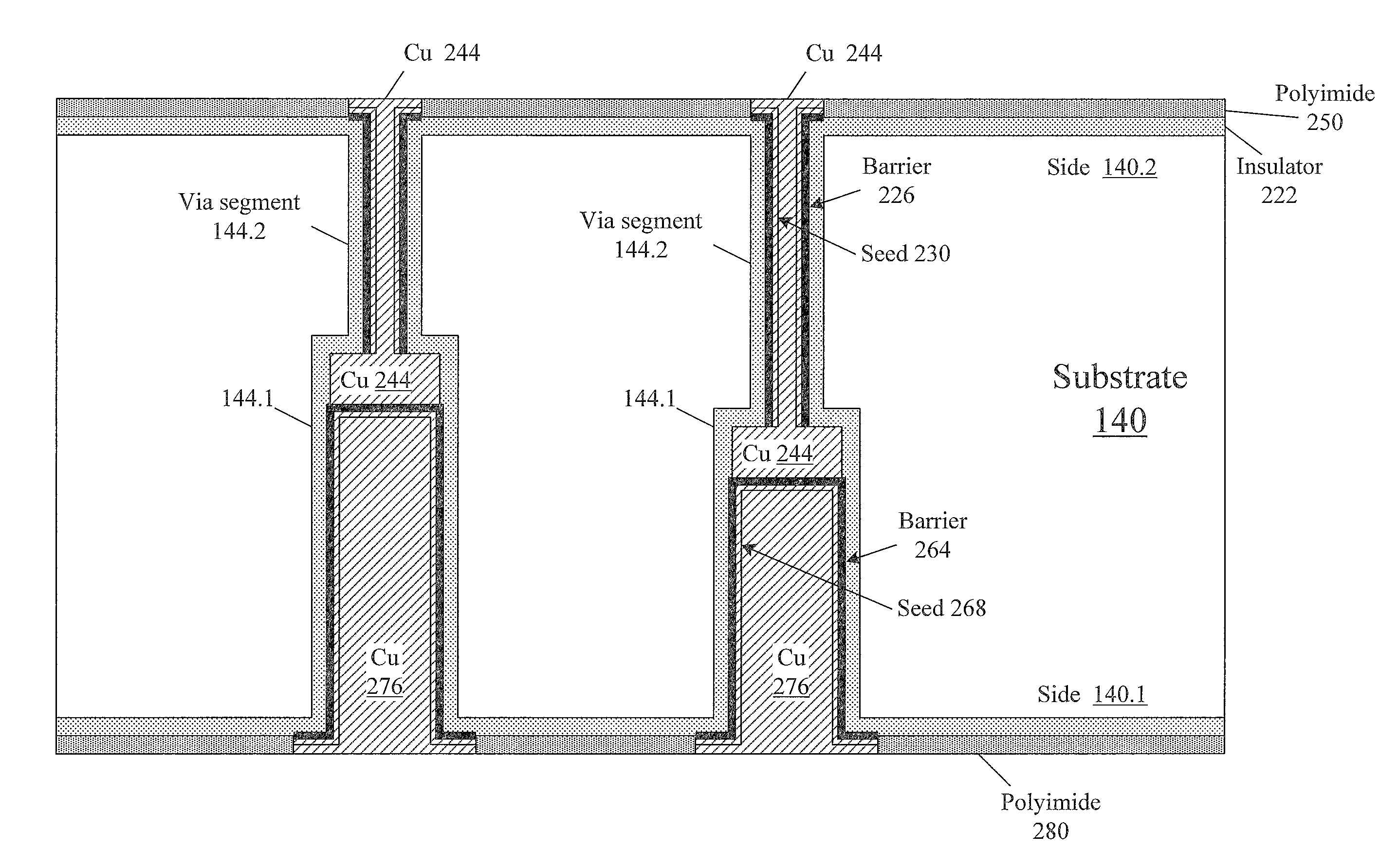
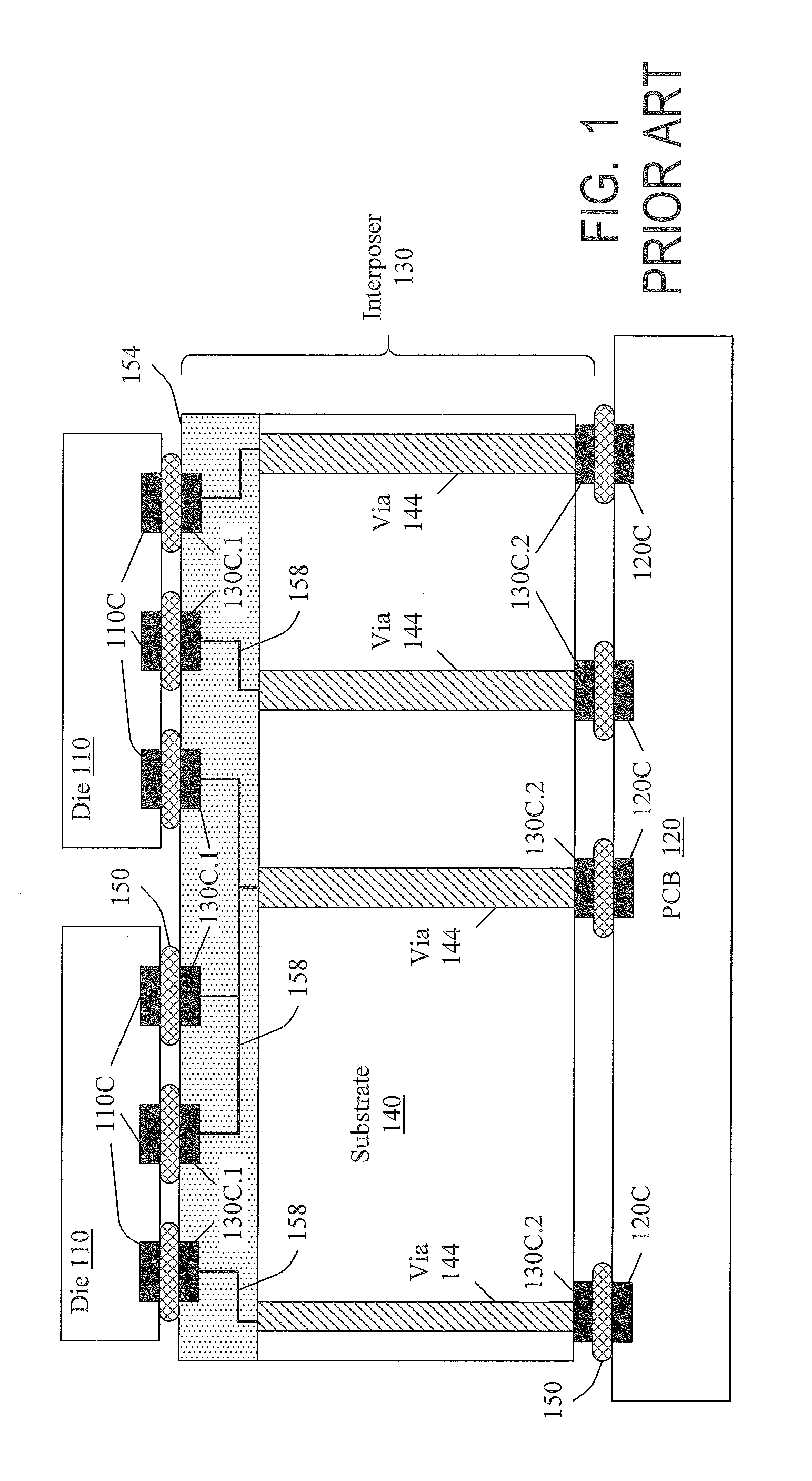
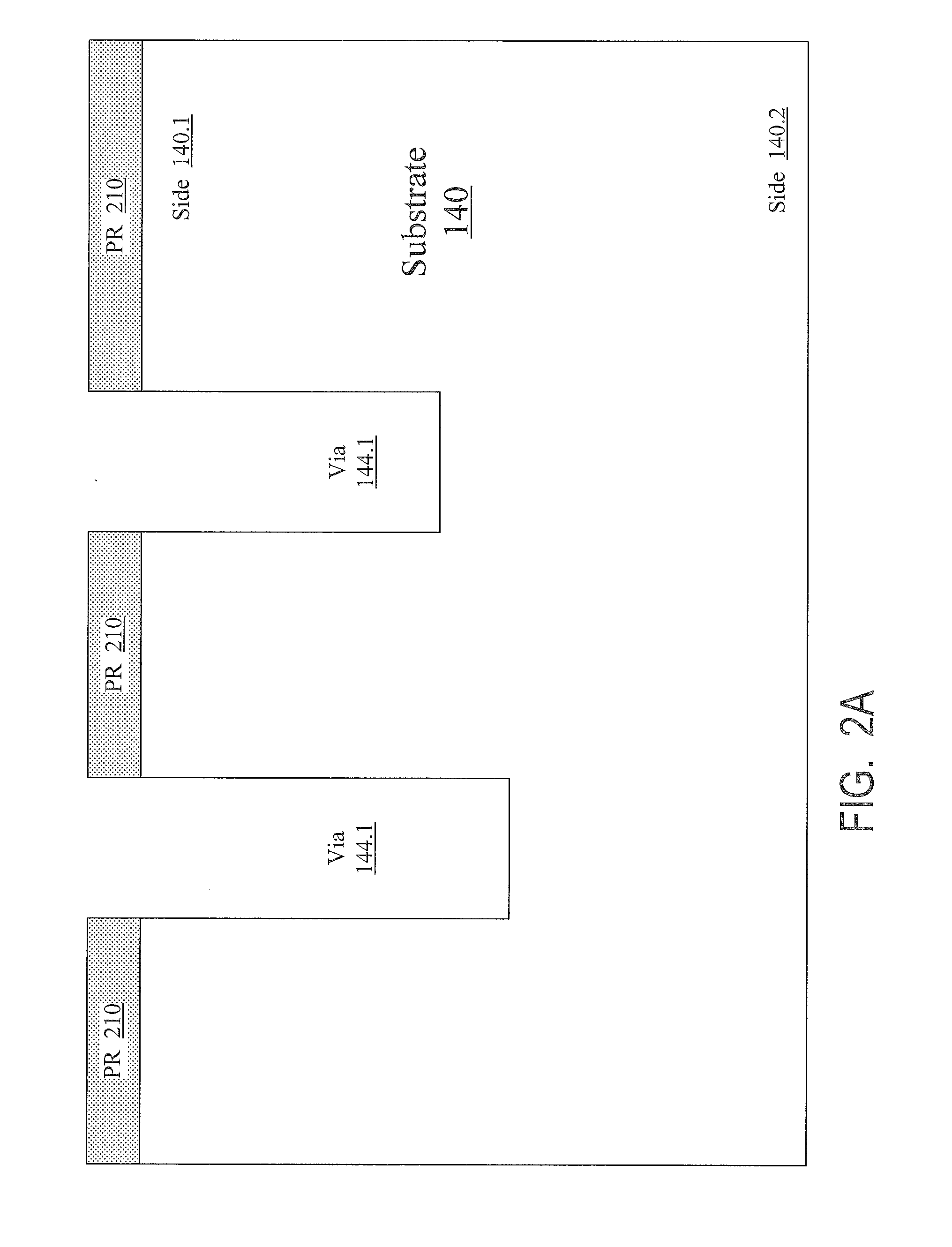
[0016]FIG. 2A illustrates the beginning stages of fabrication of metalized vias in a substrate 140 in some embodiments of the present invention. The substrate 140 can be used in an interposer 130 as in FIG. 1, to connect dies 110 to PCB 120. Substrate 140 can also be used to interconnect other structures attached to the top and bottom of the substrate, e.g. dies attached to the top to dies attached to the bottom. The structures attached to the top and bottom of substrate 140 may include other interposers. In other embodiments, substrate 140 is not an interposer but an integrated circuit not attached to any other integrated circuit. Vias 144 can be used to interconnect circuit elements at the top and bottom of substrate 140, or to connect such elements to PCB 120 or to other dies or interposers. Other uses of vias 144 may be possible.

[0017]For the...


PUM


Abstract

A through via (144) contains a conductor (244, 276) passing through a substrate (140) for connection to an integrated circuit element. The through via consists of two segments (144.1, 144.2) formed from respective different sides (140.1, 140.2) of the substrate and meeting inside the substrate. Each segment is shorter than the entire via, so via formation is facilitated. The second segment is etched after deposition of an etch stop layer (214) into the first segment. Due to the etch stop layer, the first segment's depth does not have to be rigidly controlled. The conductor is formed by separate depositions of conductive material into the via from each side of the substrate. From each side, the conductor is deposited to a shallower depth than the via depth, so the deposition is facilitated. Other embodiments are also provided.

Description

BACKGROUND OF THE INVENTION[0001]The present invention relates to integrated circuits, and more particularly to substrates having through vias with conductive features.[0002]Through vias with conductive features in a substrate are used to shorten conductive paths between circuit elements in integrated-circuit packages. For example, FIG. 1 illustrates integrated circuit dies 110 attached to a printed circuit board (PCB) 120 through an interposer 130. The interposer includes a substrate 140 with metalized through vias 144. Compared to a direct attachment of dies 110 to PCB 120, the interposer may redistribute the contact pads to reduce the package area (the area of the entire structure). More particularly, dies 110 have contact pads 110C attached to the interposer's contact pads 130C.1 by solder features 150. The interposer has contact pads 130C.2 attached to contact pads 120C of PCB 120 with other solder features 150. Many fabrication processes allow smaller critical dimensions in di...

Claims


Application Information

Patent Timeline
IPC IPC(8): H01L23/48H01L21/441
CPCH01L2924/01029H05K2203/1476H01L2924/01005H01L2924/01006H01L2924/01033H01L2924/01074H01L2924/014H01L23/481H01L24/05H05K1/0306H05K1/113H05K3/42H05K2201/09563H05K2201/09845H01L21/76898H01L2924/12042H01L21/76847H01L2924/00H01L23/49822H01L23/49827H05K1/0298H05K1/115H05K2201/0195
Inventor KOSENKO, VALENTINSAVASTIOUK, SERGEY
Owner INVENSAS CORP
Why Eureka
Try Eureka