Transistor and fabrication method thereof

Active Publication Date: 2016-05-05
SEMICON MFG INT (SHANGHAI) CORP
View PDF2 Cites 9 Cited by
  • Summary
  • Abstract
  • Description
  • Claims
  • Application Information

AI Technical Summary

Problems solved by technology

However, decreasing the gate size could cause a short channel effect, and leakage current may be generated.
Thus, the electrical properties of semiconductor devices are affected.
Therefore, there is a crystal lattice mismatch between silicon and the embedded silicon germanium structures.
At room temperature, the sma

Method used


Image

  • Transistor and fabrication method thereof
  • Transistor and fabrication method thereof
  • Transistor and fabrication method thereof

Examples


Embodiment Construction

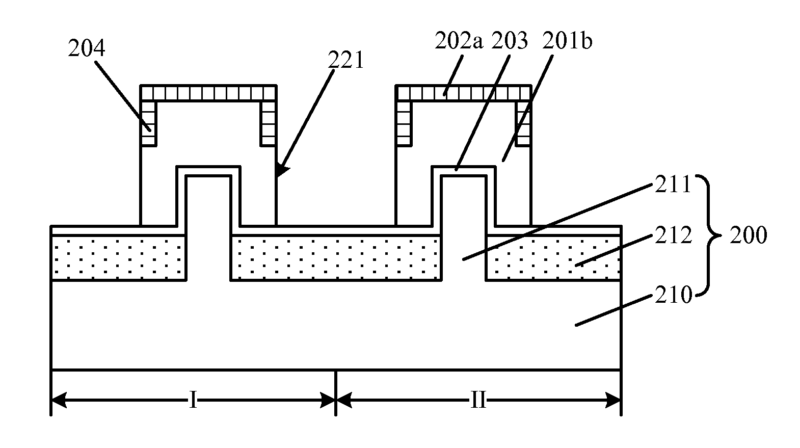
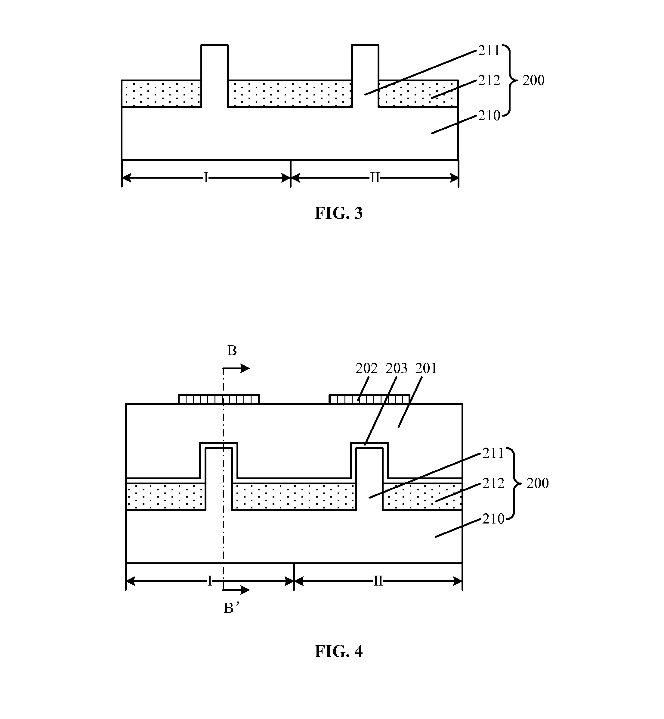
[0013]Reference will now be made in detail to exemplary embodiments of the invention, which are illustrated in the accompanying drawings. Wherever possible, the same reference numbers will be used throughout the drawings to refer to the same or like parts.

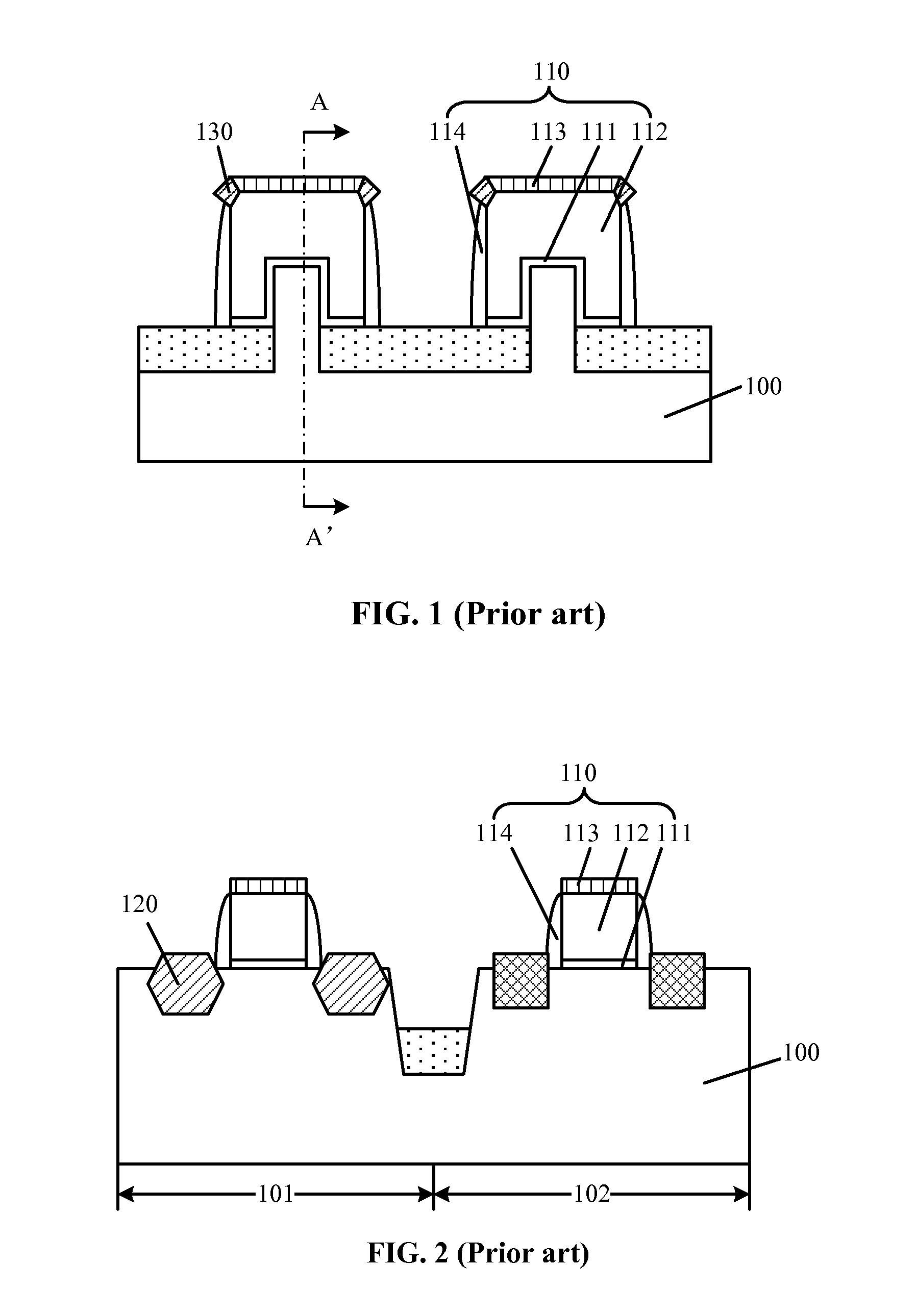
[0014]FIGS. 1˜2 illustrate an existing transistor structure having a stress layer in the source region and the drain region. FIG. 2 is the cross-sectional view of the transistor structure illustrated in FIG. 1 along the “AA′” direction.

[0015]As shown in FIGS. 1-2, the transistor structure includes a substrate 100; a plurality of gate structures 110 formed on the substrate 100. The gate structure 110 includes a gate dielectric layer 111 formed on the substrate 100; a gate layer 112 formed on the surface of the gate dielectric layer 111; a mask layer 113 formed on the surface of the gate layer 112; a sidewall spacer 114 formed on the sidewalls of the gate dielectric layer 111, the gate layer 112 and the mask layer 113; and a stress l...


PUM


Abstract

A method for forming transistors is provided. The method includes providing a substrate having a base and at least a fin on the base; and forming a gate layer on the fin, the gate layer has first side surfaces parallel to a longitudinal direction of the fin and second side surfaces perpendicular to the fin. The method also includes forming a protective layer on the first side surfaces of the gate layer to protect a vertex of the top of the gate layer from having EPI particles; and forming sidewall spacers on side surfaces of the protective layer and the second side surfaces of the gate layer. Further, the method includes forming a stress layer in the fin at both sides of the sidewall spacers and the gate layer.

Description

CROSS-REFERENCES TO RELATED APPLICATIONS[0001]This application claims the priority of Chinese patent application No. 201410599013.5, filed on Oct. 30, 2014, the entirety of which is incorporated herein by reference.FIELD OF THE INVENTION[0002]The present invention generally relates to the field of semiconductor manufacturing technology and, more particularly, to transistors and fabrication processes thereof.BACKGROUND[0003]With the rapid development of semiconductor manufacturing technology, semiconductor devices have been developed in the direction of higher component density and higher integration level. As basic semiconductor devices, transistors are currently being widely used. With the increase of the component density and integration level, the gate size of transistors has become shorter than ever. However, decreasing the gate size could cause a short channel effect, and leakage current may be generated. Thus, the electrical properties of semiconductor devices are affected. Cu...

Claims


Application Information

Patent Timeline
IPC IPC(8): H01L29/66H01L29/78
CPCH01L29/66795H01L29/7848H01L29/7851H01L29/66545H01L21/823821H01L27/0924H01L29/165H01L29/785H01L21/823431H01L27/0886
Inventor ZHAO, JIE
Owner SEMICON MFG INT (SHANGHAI) CORP
Why Eureka
Try Eureka