

Method and system for determining optical properties of semiconductor wafers
a technology of optical properties and semiconductors, applied in the direction of semiconductor/solid-state device testing/measurement, optical radiation measurement, instruments, etc., can solve the problems of limiting the computing speed of finished microchips, non-contact optical pyrometry systems for determining temperature, and systems measuring an apparent temperature rather than the true temperature of wafers, so as to improve accuracy and wafer temperature readings, improve measurement and/or prediction of thermal radiative properties of substrates, and accurate heat the
- Summary
- Abstract
- Description
- Claims
- Application Information
AI Technical Summary
Benefits of technology
Problems solved by technology
Method used
Image

Examples
Embodiment Construction
[0049]It is to be understood by one of ordinary skill in the art that the present discussion is a description of exemplary embodiments only, and is not intended as limiting the broader aspects of the present invention.
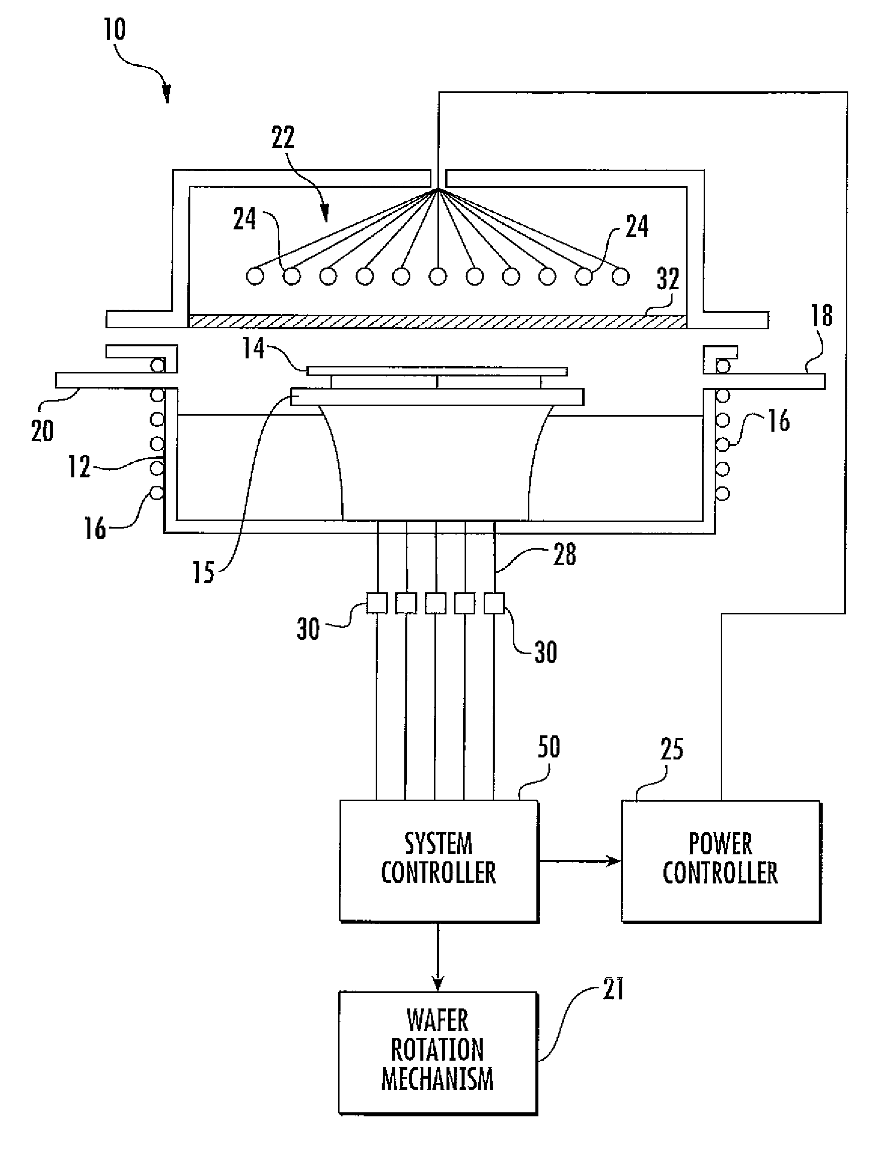
[0050]In general, the present disclosure is directed to a method and to a system for determining at least one optical characteristic of a substrate and then using the characteristic to control a process that is carried out on the substrate. For example, in one embodiment, the substrate may comprise a semiconductor wafer and the optical characteristic is used to better determine and control the temperature of the wafer during a heating process. Alternatively, the optical characteristic may be used to control a heating device that is used to heat the wafer.
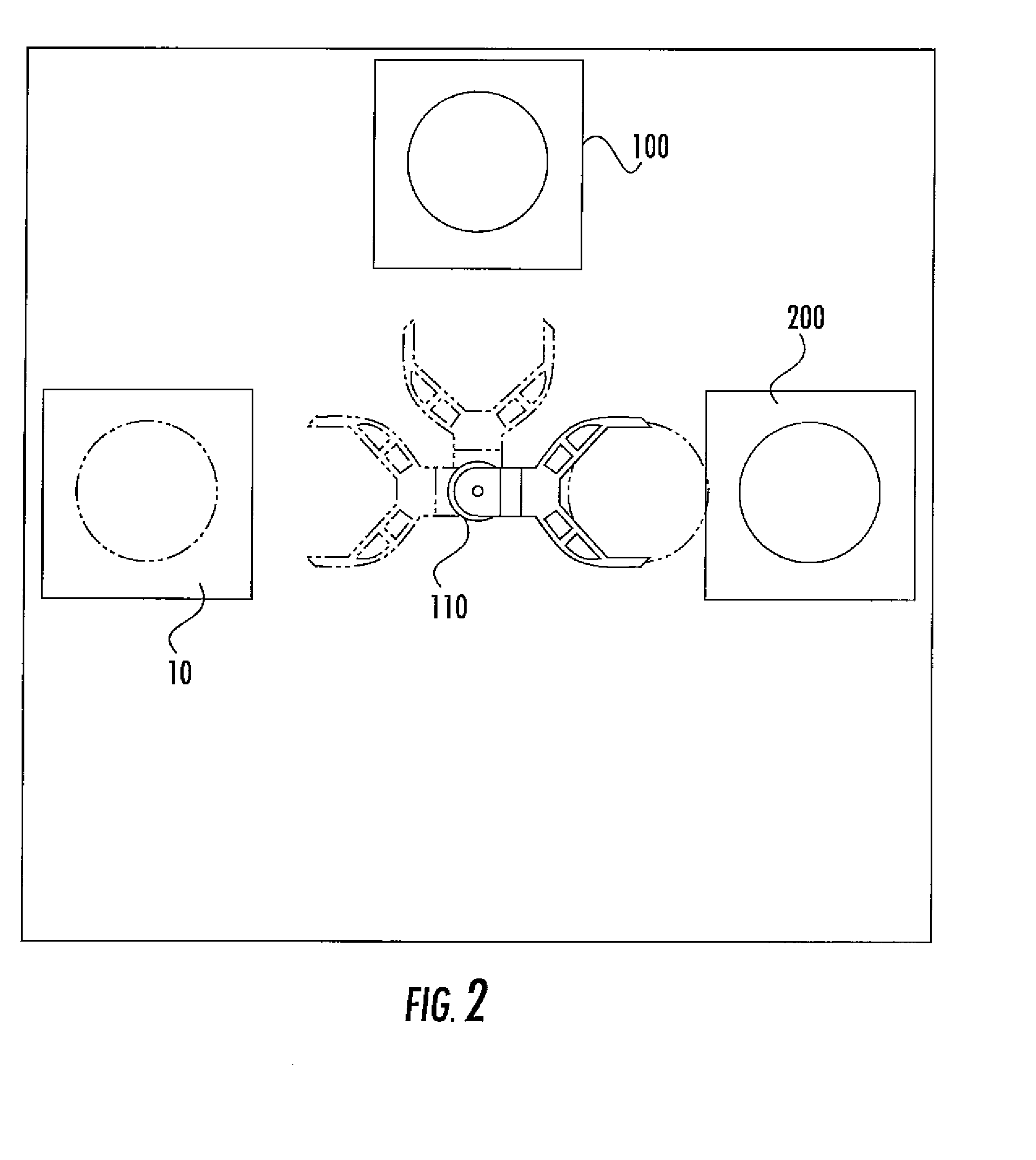
[0051]It should be understood, that the methods of the present disclosure may be used in conjunction with other substrates in addition to semiconductor wafers. For instance, the methods of the present disclosure may be...
PUM
 Abstract
Description
Claims
Application Information