Multistack solder wafer filling

a multi-stack solder wafer and soldering technology, applied in the direction of manufacturing tools, non-electric welding apparatus, soldering apparatus, etc., can solve the problems of limited use of solder for interconnection, high cost and time-consuming process of providing conductive interconnection structures for such multistacks

Inactive Publication Date: 2012-09-20
IBM CORP
View PDF3 Cites 9 Cited by
  • Summary
  • Abstract
  • Description
  • Claims
  • Application Information

AI Technical Summary

Benefits of technology

[0006]In an embodiment of the present invention, a plurality of through-substrate holes is formed in at least one substrate. Each through-substrate hole extends from a top surface of the at least one substrate to the bottom surface of the at least one substrate. The at least one substrate is held by a stationary chuck or a rotating chuck. Vacuum suction is provided to a set of through-substrate holes among the plurality of through-substrate holes through a vacuum manifold attached to the bottom surface of the at least one substrate. An injection mold solder head located above the top surface of the at least one substrate injects a solder material into the set of through-substrate holes to form a plurality of through-substrate solders that extend from the top surface to the bottom surface of the at least one substrate. The vacuum suction prevents formation of air bubbles or incomplete filling in the plurality of through-substrate holes.

Problems solved by technology

Such vertically stacked substrates are typically called “multistacks.” Providing conductive interconnect structures for such multistacks is a costly and time-consuming process.
As such, any use of solder for interconnection is limited to the space between two substrates but not extending into any of the two substrates.

Method used


Image

  • Multistack solder wafer filling
  • Multistack solder wafer filling
  • Multistack solder wafer filling

Examples


first embodiment

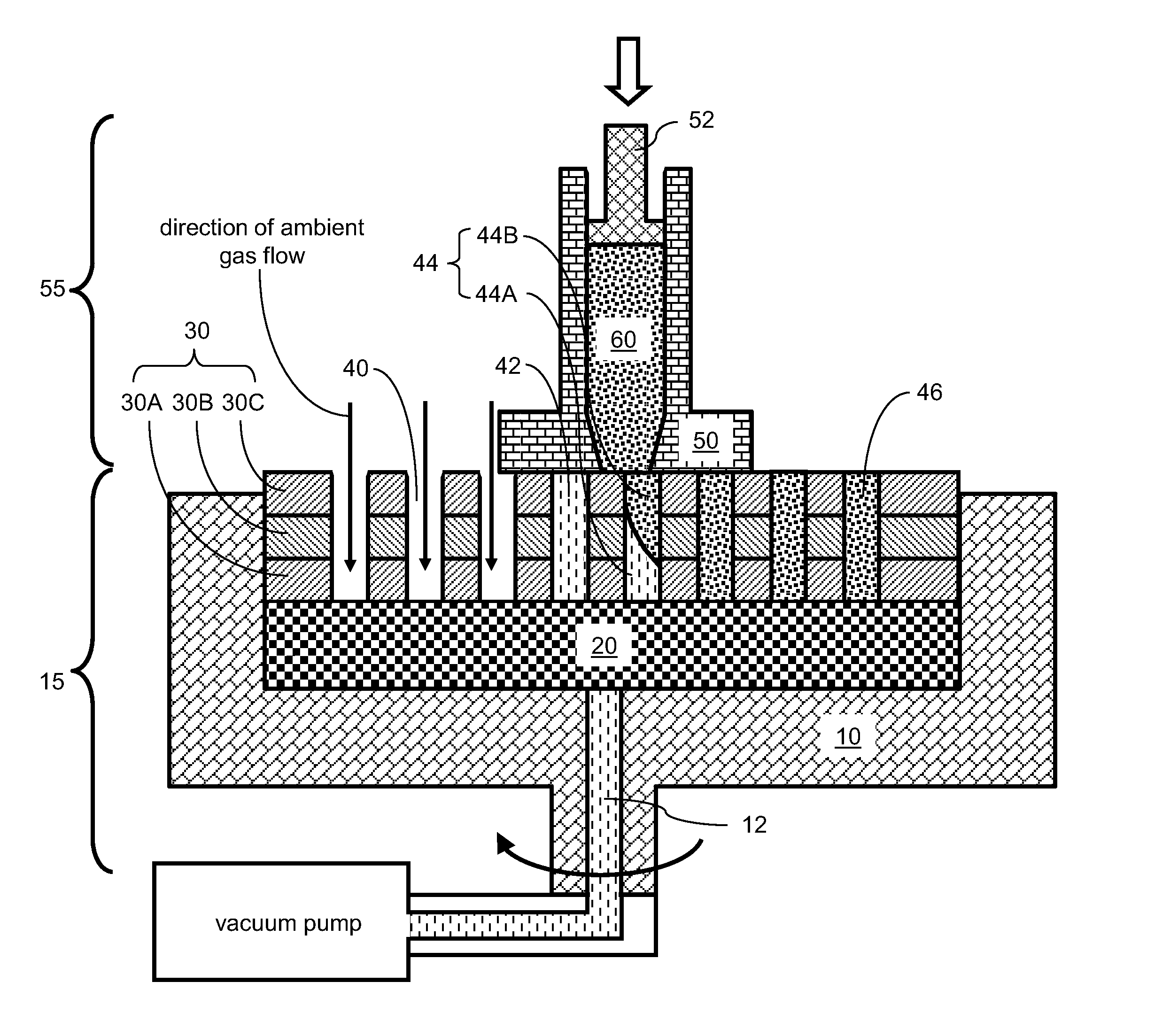
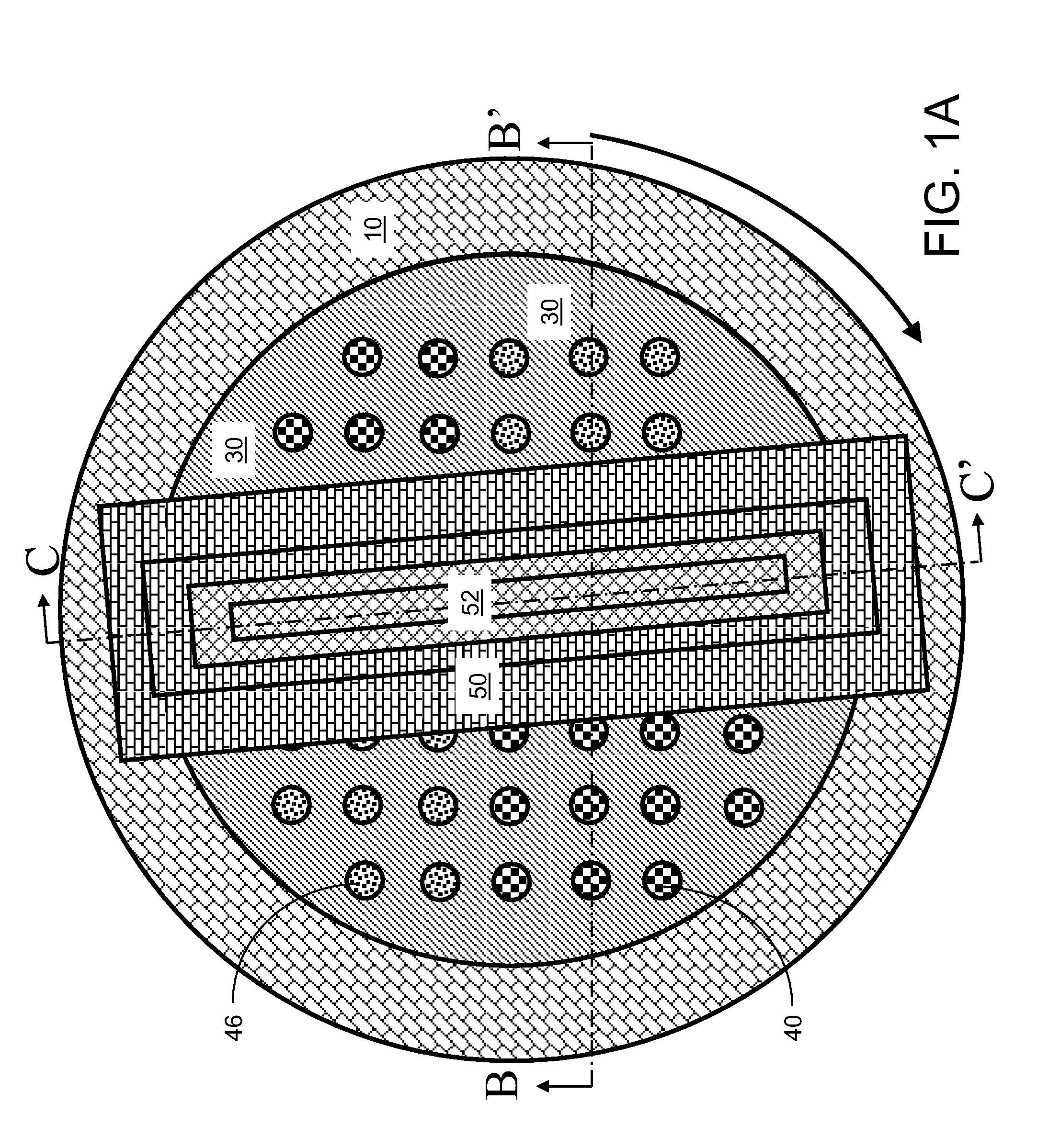
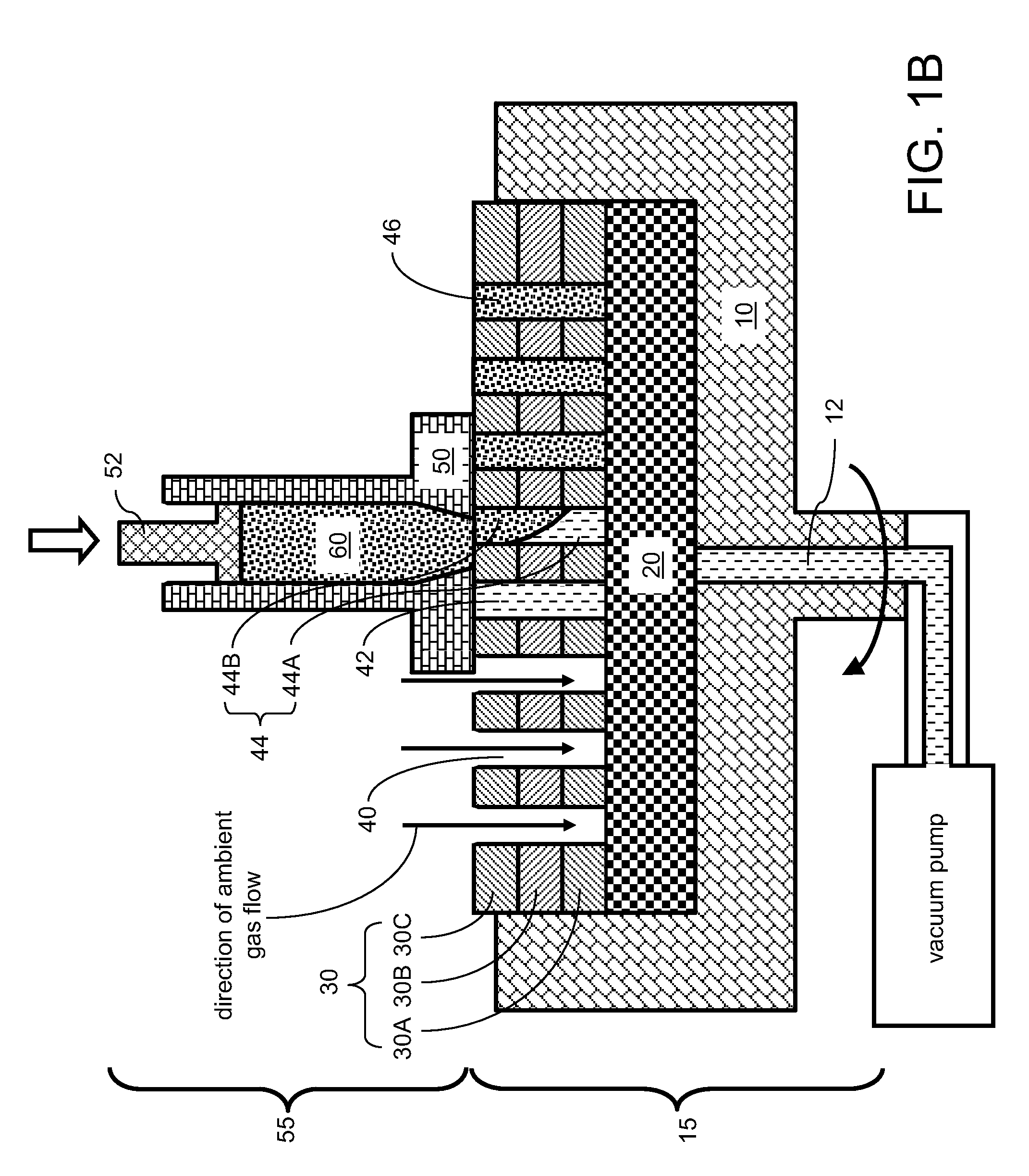
[0024]Referring to FIGS. 1A-1C, a first exemplary apparatus according to the present invention is shown, which can be employed to form at least one seamless conductive solder structure through at least one substrate 30. The first exemplary apparatus includes an upper assembly 55, a lower assembly 15, and a vacuum pump (not shown). The upper assembly 55 and the lower assembly 15 are configured to move relative to each other. The lower assembly 15 is configured to hold the at least one substrate 30, which may include, for example, a stack of a first substrate 30A, a second substrate 30B, and a third substrate 30C. While the present invention is illustrated employing the at least one substrate 30 that includes the first, second, and third substrates (30A, 30B, 30C) that are vertically stacked, the present invention can be employed for a single substrate or a plurality of substrates of any number that are vertically stacked together.

[0025]Each of the at least one substrate (30A, 30B, 30...

second embodiment

[0042]Referring to FIG. 2, a second exemplary apparatus according to the present invention includes the same elements as the first exemplary apparatus described above with a difference that the upper assembly 55 (See FIGS. 1B and 1C) and / or the lower assembly 15 (See FIGS. 1B and 1C) move relative to each other in a one-dimensional linear motion or in a two-dimensional linear motion. Preferably, the relative motion is designed to provide filling of all through substrate holes in the at least one substrate 30.

third embodiment

[0043]Referring to FIGS. 3A-3C, a third exemplary apparatus according to the present invention is shown, which can be employed to form at least one seamless conductive solder structure through at least one substrate 30. The third exemplary apparatus includes a set of an upper assembly 155 and a lower assembly 125, a middle assembly 105, and a vacuum pump (not shown). The middle assembly 105 and the set of the upper and lower assemblies (155, 125) are configured to move relative to each other while the upper assembly 155 maintains a same relative position with respect to the lower assembly 125. Thus, in a frame of reference that moves with the upper assembly, the lower assembly 125 looks stationary, while the middle assembly 105 moves relative to the upper assembly 155.

[0044]The middle assembly 105 includes a first chuck 110 that is configured to laterally confine at least one substrate 30. Further, the first chuck 110 is configured to maintain a same relative position with respect t...


PUM

PropertyMeasurementUnit
melting pointaaaaaaaaaa
conductiveaaaaaaaaaa
timeaaaaaaaaaa

Abstract

A plurality of through-substrate holes is formed in each of at least one substrate. Each through-substrate hole extends from a top surface of the at least one substrate to the bottom surface of the at least one substrate. The at least one substrate is held by a stationary chuck or a rotating chuck. Vacuum suction is provided to a set of through-substrate holes among the plurality of through-substrate holes through a vacuum manifold attached to the bottom surface of the at least one substrate. An injection mold solder head located above the top surface of the at least one substrate injects a solder material into the set of through-substrate holes to form a plurality of through-substrate solders that extend from the top surface to the bottom surface of the at least one substrate. The vacuum suction prevents formation of air bubbles or incomplete filling in the plurality of through-substrate holes.

Description

CROSS REFERENCE TO RELATED APPLICATION[0001]This application is a divisional of U.S. patent application Ser. No. 12 / 571,965, filed Oct. 1, 2009 the entire content and disclosure of which is incorporated herein by reference.BACKGROUND[0002]The present invention generally relates to apparatuses and methods for forming seamless solder structures through at least one substrate.[0003]As consumer products such as mobile phones become thinner, highly integrated semiconductor chips are needed to provide multiple functions within a single portable device. In such devices, power and ground interconnects as well as signal interconnects extend not only across a single substrate including a semiconductor chip, but also across multiple substrates that include multiple semiconductor chips that are vertically stacked. Such vertically stacked substrates are typically called “multistacks.” Providing conductive interconnect structures for such multistacks is a costly and time-consuming process.[0004]T...

Claims


Application Information

Patent Timeline
Patent Type & Authority Applications(United States)
IPC IPC(8): B23K31/02B23K3/06
CPCB23K1/0016B23K2201/40B23K3/0638B23K2101/40
Inventor CHEY, S. JAYDANOVITCH, DAVIDGRUBER, PETER A.TSANG, CORNELIA K.
Owner IBM CORP
Why Eureka
Try Eureka