Control of Local Environment for Polysilicon Conductors in Integrated Circuits

a technology of integrated circuits and local environment, applied in the direction of basic electric elements, electrical apparatus, semiconductor devices, etc., can solve the problems of difficult control of critical dimensions and resolution, and achieve the effect of improving photolithography

Active Publication Date: 2012-09-20
TEXAS INSTR INC
View PDF4 Cites 2 Cited by
  • Summary
  • Abstract
  • Description
  • Claims
  • Application Information

AI Technical Summary

Benefits of technology

[0009]Embodiments of this invention provide an integrated circuit and method of fabricating the same having improved photolithography process margin for minimum feature size (i.e., critical dimension) interconnections over isolation structures.

Problems solved by technology

The masked patterning of features having dimensions smaller than the wavelength of the incident light has raised many complex issues in the photolithography process.
But because the regularity of pitch and preferred orientation rules cannot be obeyed for these field poly interconnects and other structures, resolution and critical dimension control is rendered difficult.

Method used


Image

  • Control of Local Environment for Polysilicon Conductors in Integrated Circuits
  • Control of Local Environment for Polysilicon Conductors in Integrated Circuits
  • Control of Local Environment for Polysilicon Conductors in Integrated Circuits

Examples


Embodiment Construction

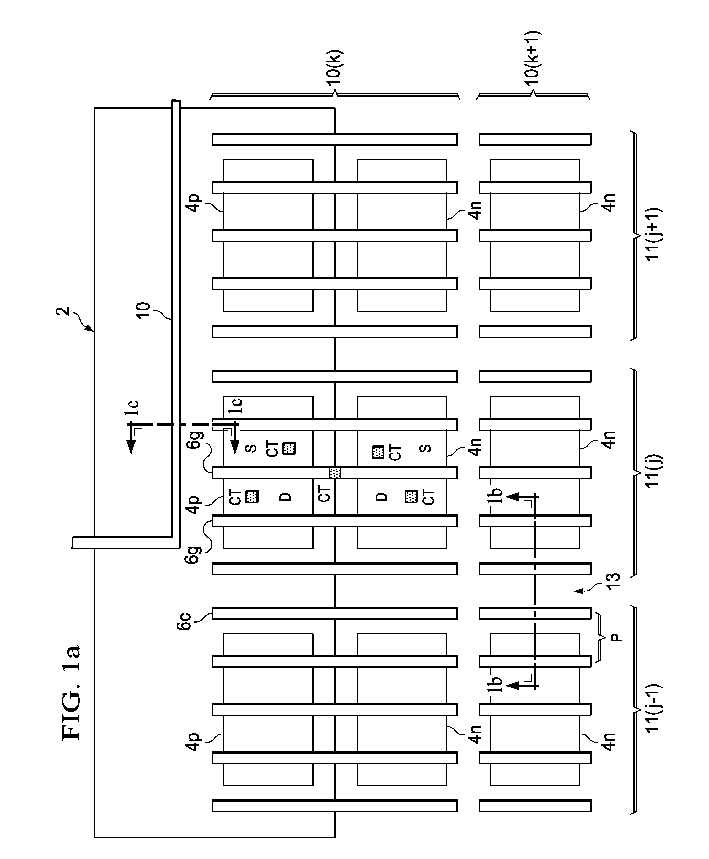
[0019]This invention will be described in connection with one or more of its embodiments, namely as implemented into a metal-oxide-semiconductor (MOS) integrated circuit in which active areas are arranged in regular blocks, because it is contemplated that this invention will be especially beneficial in such an application. However, it is also contemplated that this invention may provide advantages and benefits in other integrated circuit applications. Accordingly, it is to be understood that the following description is provided by way of example only, and is not intended to limit the true scope of this invention as claimed.

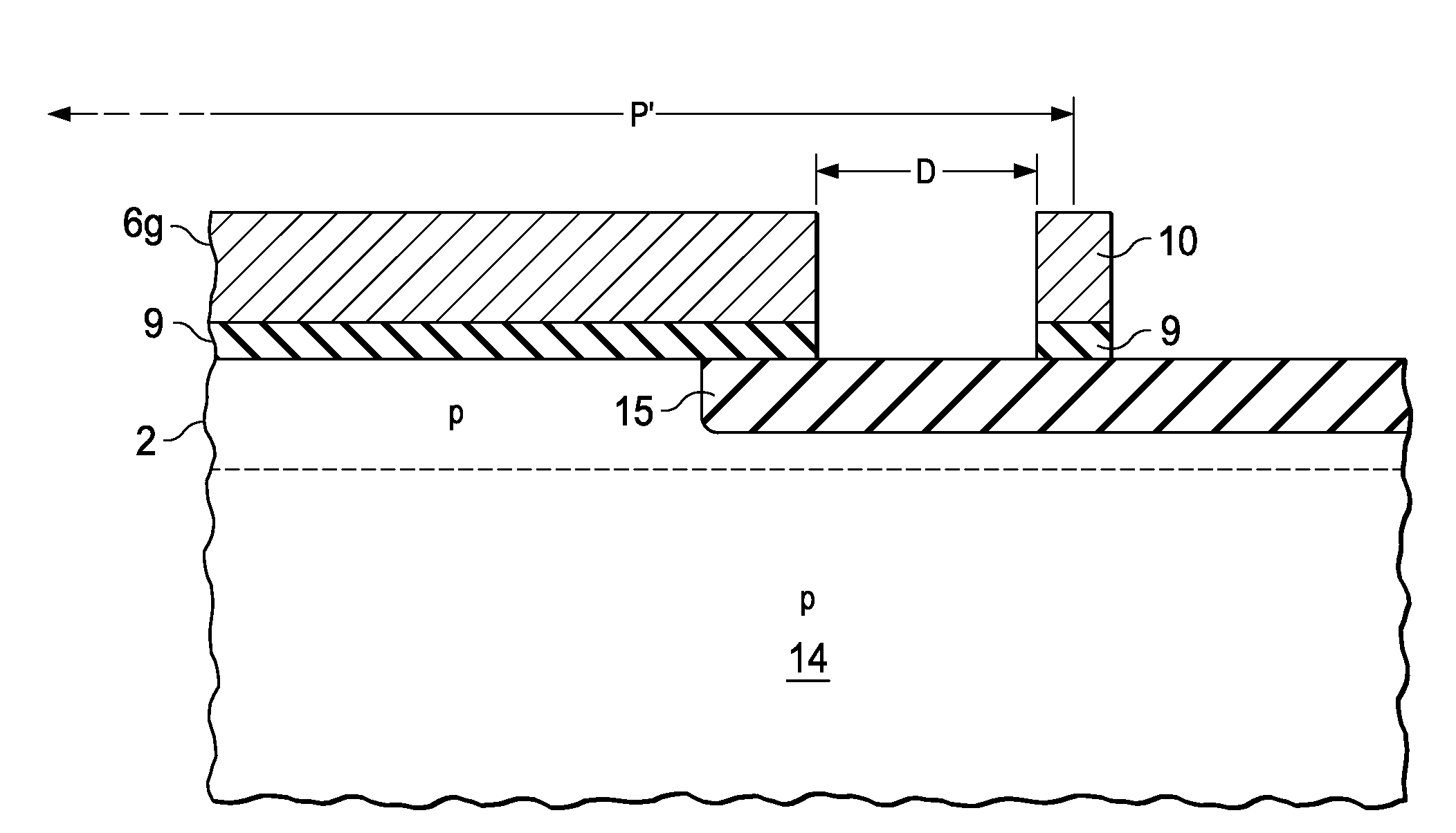
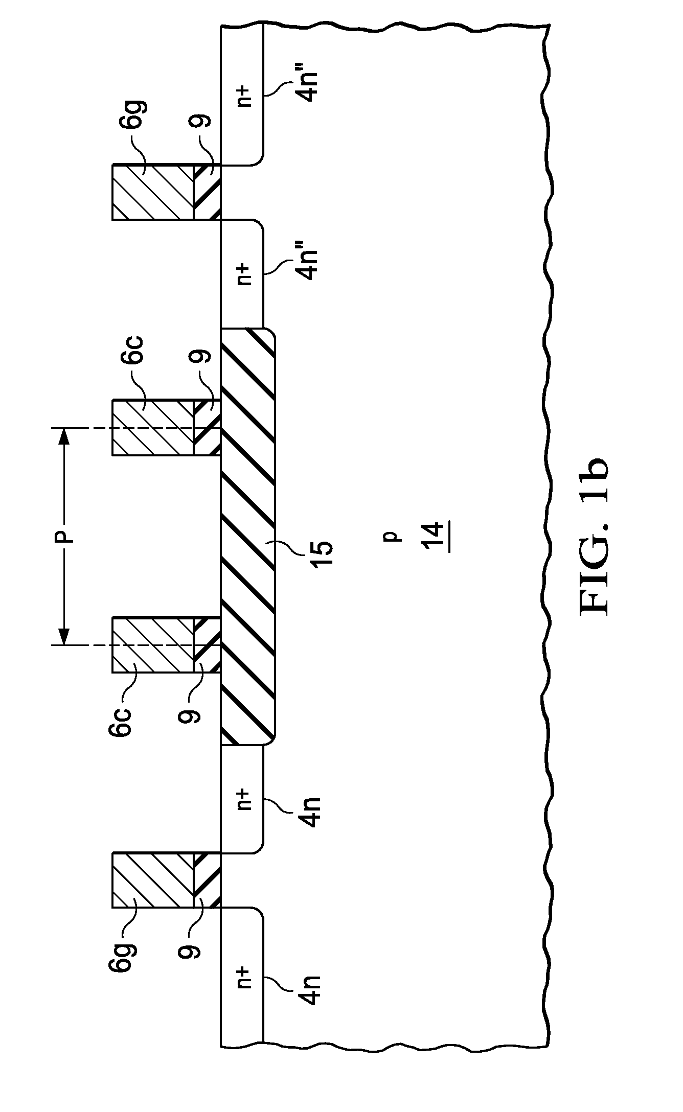
[0020]Embodiments of this invention are particularly useful in connection with the manufacture of modern MOS integrated circuits in which the smallest features to be defined by way of optical photolithography are of a size less than 100 nm, and especially in such integrated circuits in which these patterned features are smaller than 50 nm. In particular, embodime...


PUM


Abstract

A method of fabricating gate level electrodes and interconnects in an integrated circuit, and an integrated circuit so fabricated, with improved process margin for the gate level interconnects of a width near the critical dimension. Off-axis illumination, as used in the photolithography of deep sub-micron critical dimension, is facilitated by the patterned features having a preferred orientation in a common direction, with a pitch constrained to within a relatively narrow range. Interconnects in that same gate level, for example “field poly” interconnects, that run parallel to an array of gate elements are placed within a specified distance range from the ends of the gate elements, or at a distance sufficient to allow sub-resolution assist features.

Description

CROSS-REFERENCE TO RELATED APPLICATIONS[0001]Not applicable.STATEMENT REGARDING FEDERALLY SPONSORED RESEARCH OR DEVELOPMENT[0002]Not applicable.BACKGROUND OF THE INVENTION[0003]This invention is in the field of integrated circuit manufacture. Embodiments of this invention are directed to the physical layout of polysilicon conductors at locations of integrated circuits away from active transistor regions.[0004]Advances in semiconductor technology in recent years have enabled the shrinking of minimum device feature sizes, such as metal-oxide-semiconductor (MOS) transistor gates, into the deep sub-micron range. For example, according to some advanced manufacturing technologies as of this date, the target MOS transistor gate width after etch is on the order of 30 nm. Because of the strong effect of transistor channel length on the overall performance of the integrated circuit, as well as on the chip area required for fabrication of a given circuit function, the dimension of transistor g...

Claims


Application Information

Patent Timeline
Patent Type & Authority Applications(United States)
IPC IPC(8): H01L27/04H01L21/336
CPCH01L21/823828H01L27/0207H01L29/78H01L21/28123H01L29/66484
Inventor BLATCHFORD, JR., JAMES WALTERCHOI, YONG SEOK
Owner TEXAS INSTR INC
Why Eureka
Try Eureka