High density resistance based semiconductor device

a technology of resistance and semiconductor devices, applied in semiconductor devices, digital storage, instruments, etc., can solve problems such as problems in manufacturing devices with very small dimensions

Active Publication Date: 2011-12-06
MACRONIX INT CO LTD
View PDF22 Cites 3 Cited by
  • Summary
  • Abstract
  • Description
  • Claims
  • Application Information

AI Technical Summary

Benefits of technology

[0011]Memory arrays having memory cells as described herein result in high density memory and provide multi-level operation. In embodiments the cross-sectional area of the memory cells of the array is determined by dimensions of word lines and bit lines, allowing for a high density for the array. The word lines have word line widths and adjacent word lines are separated by a word line separation distance, and the bit lines have bit line widths and adjacent bit lines are separated by a bit line separation distance. In preferred embodiments the summation of the word line width and the word line separation distance is equal to twice a feature size F used to form the array, and the summation of the bit line width and the bit line separation distance is equal to twice the feature size F. Additionally, F is preferably a minimum feature size for a process (typically a lithographic process) used to form the bit lines and word lines, such that the memory cells of the array have a memory cell area of 4 F2.

Problems solved by technology

However, problems have arisen in manufacturing devices with very small dimensions, and with variations in manufacturing processes needed to meet the tight tolerance requirements necessary for large-scale high-density memory devices.

Method used


Image

  • High density resistance based semiconductor device
  • High density resistance based semiconductor device
  • High density resistance based semiconductor device

Examples


Embodiment Construction

[0021]The following description of the invention will typically be with reference to specific structural embodiments and methods. It is to be understood that there is no intention to limit the invention to the specifically disclosed embodiments and methods but that the invention may be practiced using other features, elements, methods and embodiments. Preferred embodiments are described to illustrate the present invention, not to limit its scope, which is defined by the claims. Those of ordinary skill in the art will recognize a variety of equivalent variations on the description that follows. Like elements in various embodiments are commonly referred to with like reference numerals.

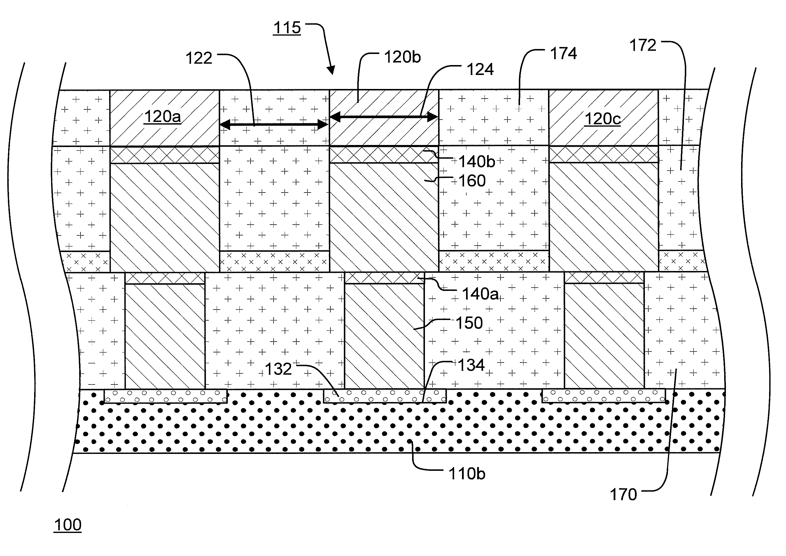
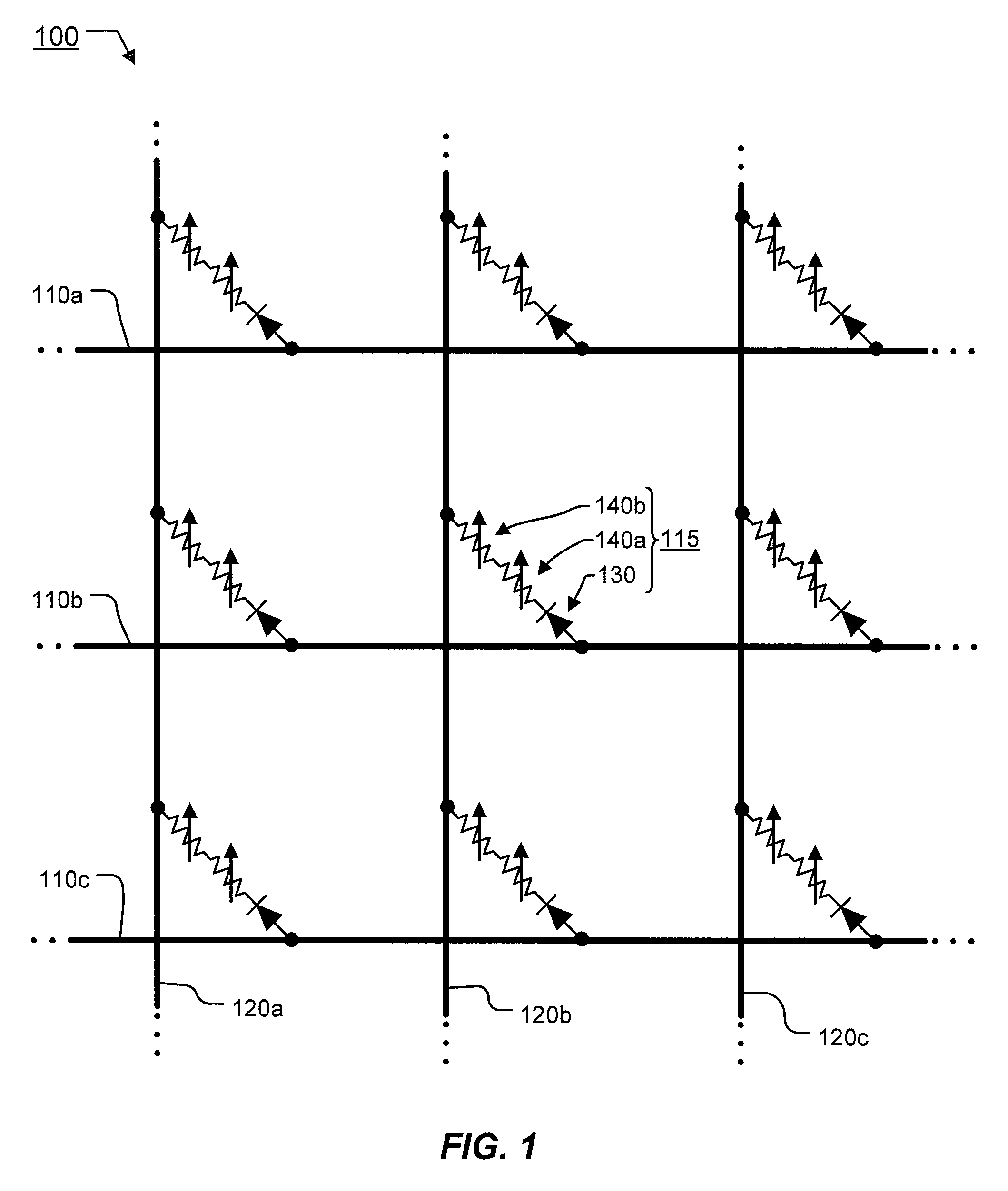
[0022]FIG. 1 illustrates a schematic diagram of a portion of a cross-point memory array 100 implemented using three-dimensional memory cells as described herein, each memory cell having a plurality of metal-oxide based memory elements and a diode access device. In FIG. 1, each memory cell includes two me...


PUM


Abstract

Memory devices are described along with methods for manufacturing. A memory device as described herein includes a plurality of memory cells located between word lines and bit lines. Each memory cell comprises a diode and a plurality of memory elements each comprising one or more metal-oxygen compounds, the diode and the plurality of memory elements arranged in electrical series along a current path between a corresponding word line and a corresponding bit line.

Description

BACKGROUND OF THE INVENTION[0001]1. Field of the Invention[0002]The present invention relates to memory devices and methods for manufacturing memory devices, and more particularly to high density three-dimensional (3D) memory devices having a plurality of programmable resistive memory elements based on metal-oxygen compounds.[0003]2. Description of Related Art[0004]Metal oxide based nonvolatile resistive random access memory RRAM has attracted much attention because of its simple structure and excellent properties such as low power, high speed, and a large memory window between resistive states.[0005]Tungsten-oxygen WOx based RRAM can be caused to change resistance between two or more stable ranges by application of electrical pulses at levels suitable for implementation in integrated circuits, and the resistance can be read and written with random access to indicate stored data. See, U.S. patent application Ser. No. 11 / 955,137 entitled “Memory Devices Having an Embedded Resistance ...

Claims


Application Information

Patent Timeline
Patent Type & Authority Patents(United States)
IPC IPC(8): G11C11/00
CPCG11C11/5685G11C13/0007G11C13/003H01L27/2409H01L27/2463G11C2213/32G11C2213/34G11C2213/72G11C2213/76G11C2213/78H01L45/04H01L45/1233H01L45/146H01L45/147H01L45/1633H10B63/20H10B63/80H10N70/20H10N70/826H10N70/8833H10N70/8836H10N70/028
Inventor LEE, MING-DAOULAI, ERH-KUNHSIEH, KUANG YEU
Owner MACRONIX INT CO LTD
Why Eureka
Try Eureka