Electromagnetic interference shielding structure and manufacturing method thereof

a technology of electromagnetic interference and shielding structure, which is applied in the direction of magnetic/electric field screening, localised screening, basic electric elements, etc., can solve the problems of increased manufacturing cost and non-ideal electromagnetic shielding efficiency, and achieve the effect of increasing electromagnetic interference shielding efficiency

a technology of electromagnetic interference and shielding structure, which is applied in the direction of magnetic/electric field screening, localised screening, basic electric elements, etc., can solve the problems of increased manufacturing cost and non-ideal electromagnetic shielding efficiency, and achieve the effect of increasing electromagnetic interference shielding efficiency

US20120243199A1Active Publication Date: 2012-09-27UNIVERSAL SCIENTIFIC INDUSTRIAL (SHANGHAI) CO LTD +1

Image

  • Electromagnetic interference shielding structure and manufacturing method thereof
  • Electromagnetic interference shielding structure and manufacturing method thereof
  • Electromagnetic interference shielding structure and manufacturing method thereof

Examples


Embodiment Construction

[0019]The aforementioned illustrations and following detailed descriptions are exemplary for the purpose of further explaining the scope of the present invention. Other objectives and advantages related to the present invention will be illustrated in the subsequent descriptions and appended drawings.

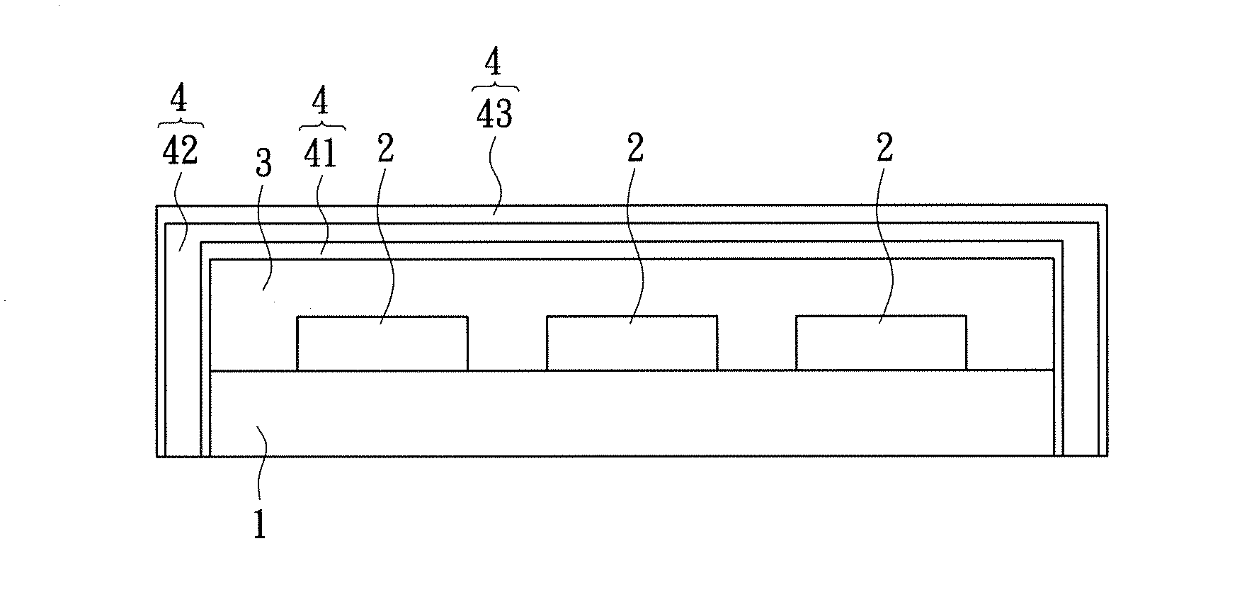
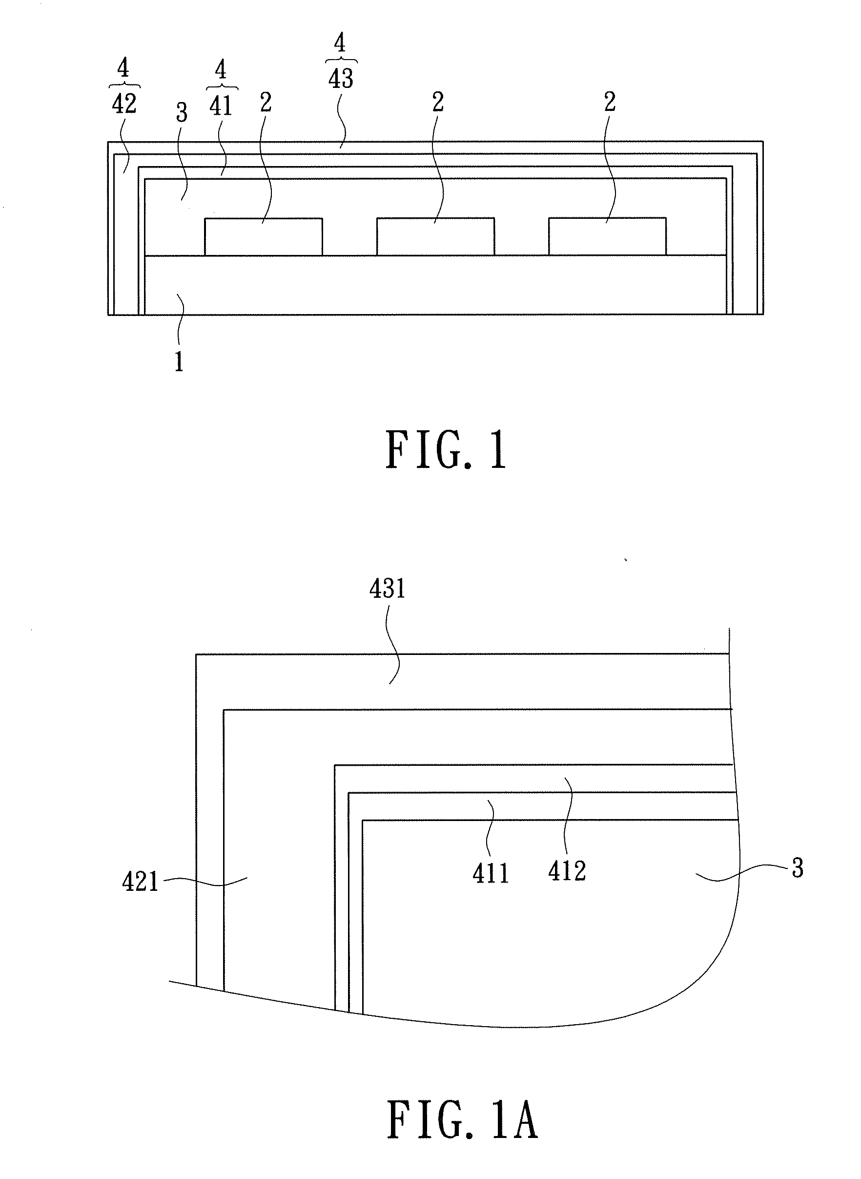
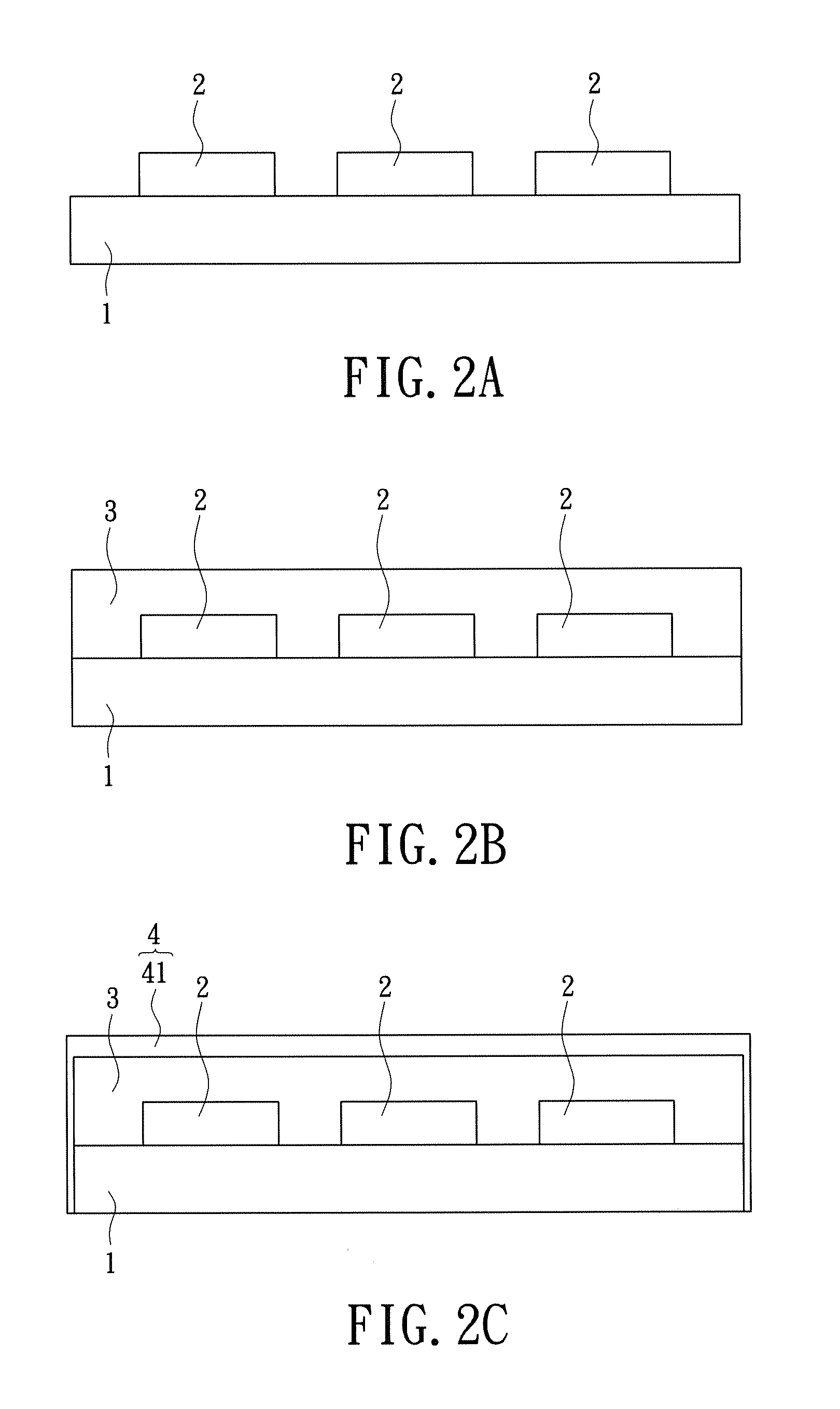
[0020]Reference FIG. 1, which shows a cross-sectional view of an electromagnetic interference (EMI) shielding structure according to an embodiment of the present invention. According to an embodiment of the present invention, the EMI shielding structure includes: a substrate 1, at least one chip unit 2, a packing layer 3, and an EMI shielding unit 4.

[0021]The substrate 1 can be a circuit board, such as a flexible printed circuit board (FPCB) or a non-flexible printed circuit board. The chip unit 2 is disposed on the surface of the substrate 1, and the chip unit 2 is electrically coupled to the substrate 1. Therein, the number of the chip unit 2 is not limited, and may depend on the produ...


PUM

PropertyMeasurementUnit
thicknessesaaaaaaaaaa

Abstract

An electromagnetic interference (EMI) shielding structure, which includes: a substrate, at least one chip unit, a packing layer, and an EMI shielding unit. The chip unit is disposed on the surface of the substrate and electrically coupled thereto. The packing layer is formed on the substrate and covers the chip unit. The EMI shielding unit includes: a first, second, and third shielding layer. The first shielding layer covers the outer surface of the packing layer and the lateral surface of the substrate. The second and third shielding layer respectively covers the outer surface of the first and second shielding layer. Based on the instant disclosure, the EMI shielding unit uses the methods of sputtering and electroless plating, to increase the adhesion strength of the EMI shielding unit and make the thickness of the shielding layer uniform. The instant disclosure raises the EMI shielding efficiency and lowers the manufacturing cost.

Description

BACKGROUND OF THE INVENTION[0001]1. Field of the Invention[0002]The present invention relates to an electromagnetic interference (EMI) shielding structure and manufacturing method thereof; in particular, to an EMI structure and manufacturing method thereof that raises the EMI shielding efficiency.[0003]2. Description of Related Art[0004]The electronic circuit components used by today's electronic products all requires electromagnetic interference (EMI) shielding structure. The primary purpose of which is to prevent the effect of electromagnetic interference from occurring between each circuit components. For each type of electronic products, only those with adequate EMI shielding structure can operate in a stable fashion with high reliability, and so as to gain the trust and loyalty of users. Therefore, for electronic fields of computer, mobile phones, transportation devise, navigation systems, household appliances, all require technology related to EMI shielding structure.[0005]Man...

Claims


Application Information

Patent Timeline
27 Sep 2012
Publication
US20120243199A1
IPC
H05K9/00; H01B19/00
CPC
H01L23/552; H05K9/003; H01L25/0655; H01L2924/0002; Y10T29/49155; Y10T29/49144; Y10T29/49227; Y10T29/49126
Inventors
WU, MING-CHE