Film forming method by sputtering apparatus and sputtering apparatus
a technology of sputtering apparatus and sputtering chamber, which is applied in the direction of electrolysis components, vacuum evaporation coatings, coatings, etc., can solve the problems of not being able to give anisotropy or the like to a film, the time until a film is formed on the whole surface of the substrate becomes long, and the non-erosion region cannot be reduced. , to achieve the effect of reducing the occurrence of non-er
- Summary
- Abstract
- Description
- Claims
- Application Information
AI Technical Summary
Benefits of technology
Problems solved by technology
Method used
Image

Examples
first embodiment
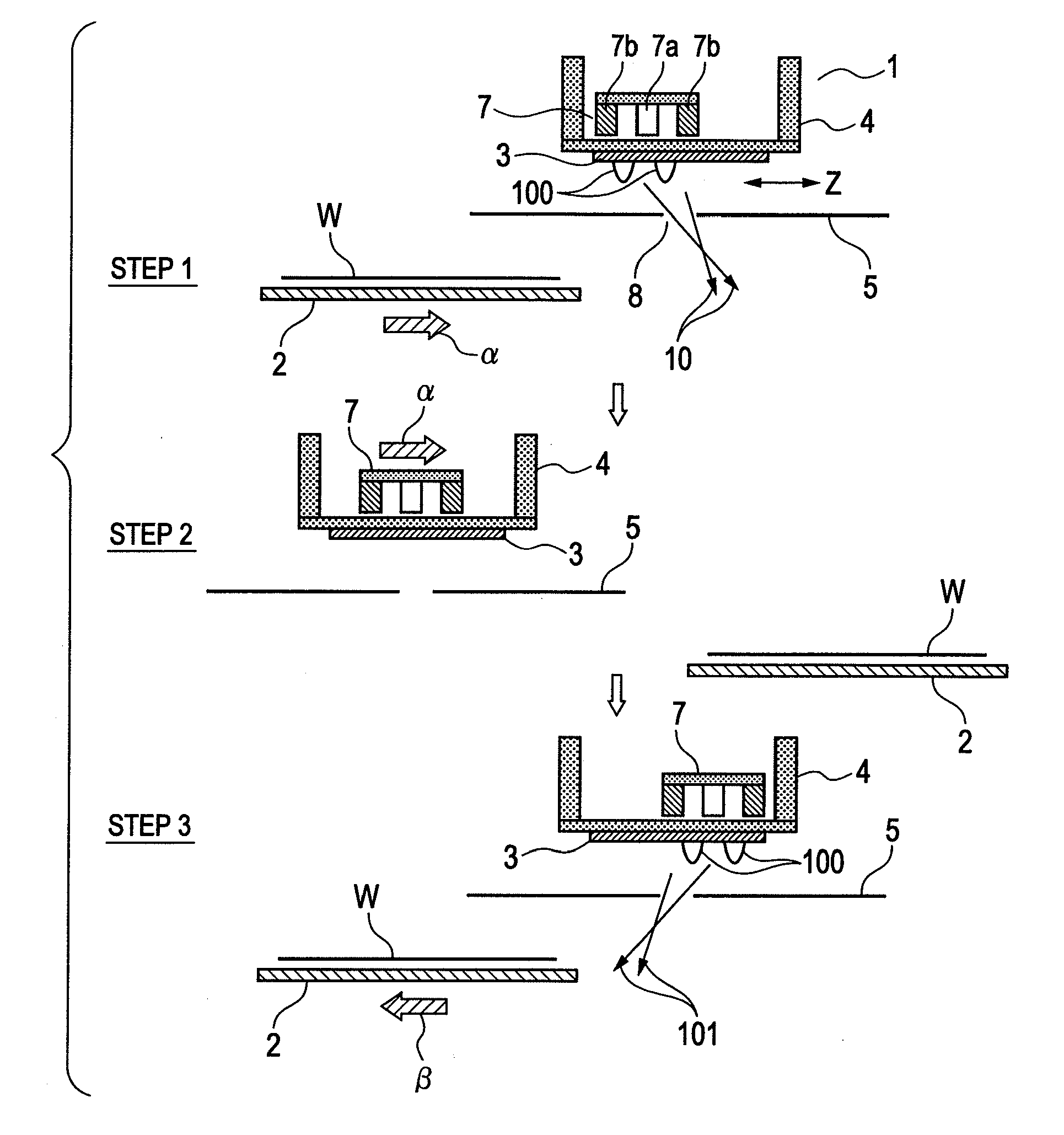
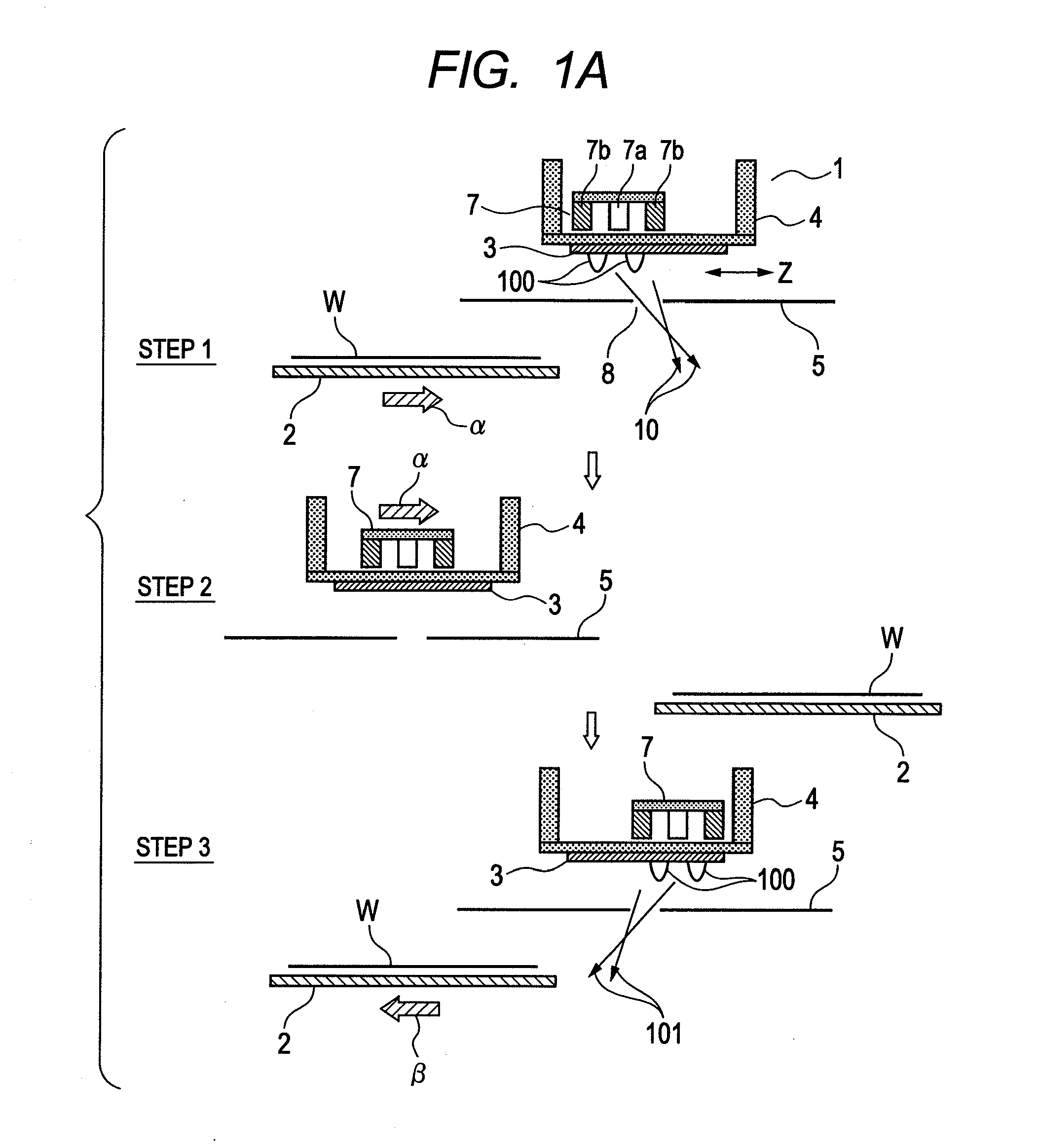
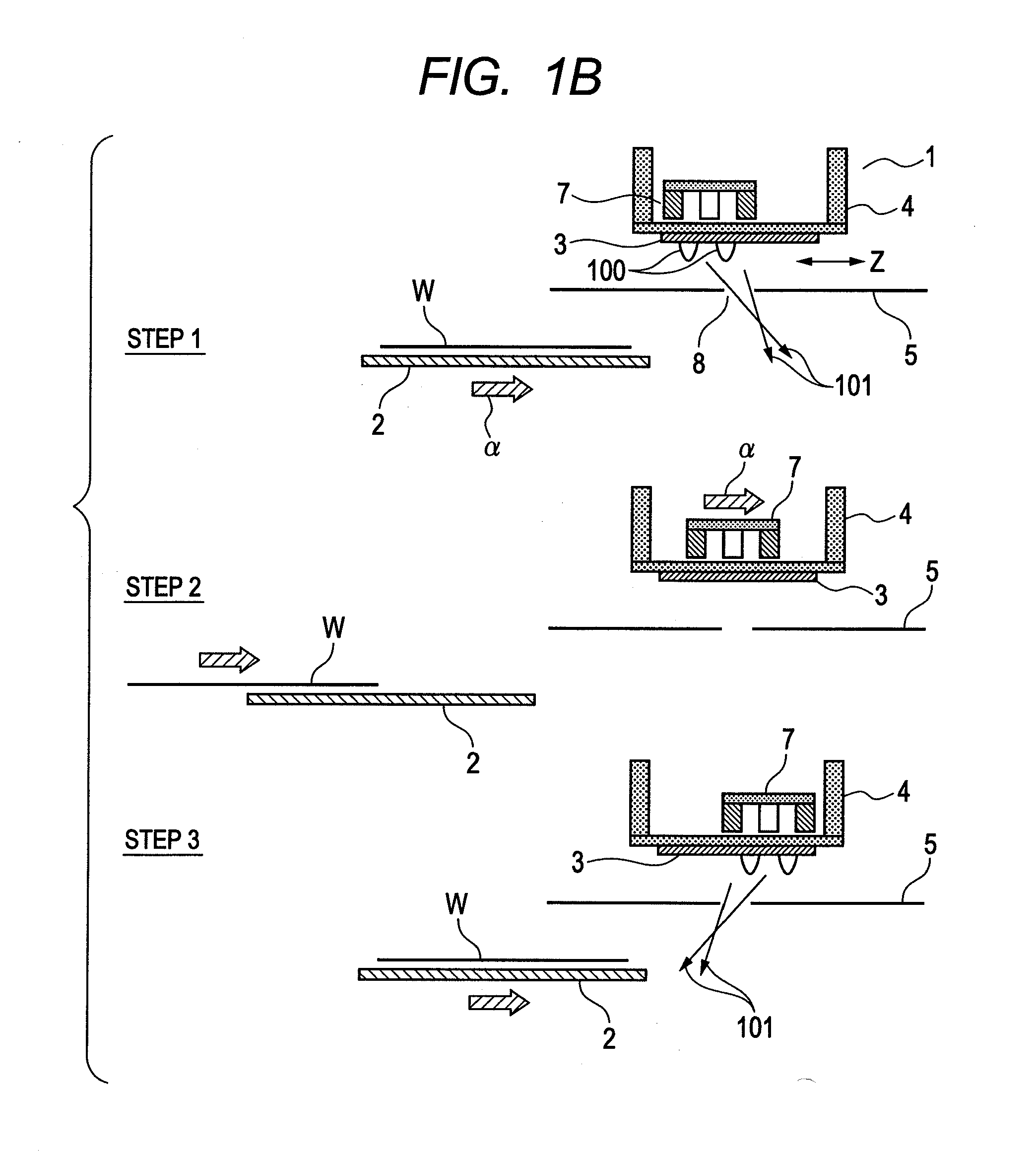
[0072]A step 1 to a step 3 in FIG. 1A are side views illustrating an example of an operation by a sputtering apparatus according to the present invention. In FIGS. 1A and 1B, the sputtering apparatus 1 includes a stage 2 as a substrate holding portion on which a substrate W can be placed, a cathode 4 capable of supporting a target 3, and a shield plate 5 having a slit-shaped opening portion (also referred to as a “slit”) 8. In FIG. 1A, the surface of the target 3 (sputter surface) and a substrate placing surface of the stage 2 are substantially parallel with each other. Therefore, the conveying direction Z can be considered as a conveying direction of the substrate when a processed surface of the substrate W (the substrate placing surface of the stage 2) and the surface of the target 3 are substantially parallel with each other.
[0073]A cathode magnet 7 is located within the cathode 4 and can move parallel with respect to the surface of the target 3 by means of a magnet driving mecha...
first example
[0121]A first example of the invention of the present application will be described. The first example is characterized by having a first step in which the cathode magnet 7 is fixed at a first position inside the cathode 4, and a film is formed on the substrate W on the substrate support surface of the stage 2, a second step in which after the film formation on the substrate W is finished, the cathode magnet 7 is moved to a second position inside the cathode 4 different from the first position and fixed, and a third step in which the film is formed on the substrate W on the substrate support surface of the stage 2 by using the cathode magnet 7 fixed at the second position.
[0122]A result by this example will be illustrated below. As in FIG. 6, a method in which the target 3 is fixed, the stage 2 is rotated, and the shield plate 5 is rotated around the rotating shaft B and a film is formed so that a film is formed while passing in front of the target 3 is exemplified. When the stage r...
second example
[0128]In order to demonstrate that the effect of the present invention is still effective even if the sputter incident angle is changed, an experiment was conducted also for the following condition as a second example:
[0129]In order to obtain
θ=60 degrees,
automatic adjustment is made so that a speed of each part is as follows:
cathode 4 0 degrees / second (stand-still)stage 21.3 degrees / secondshield plate 5θ = 60
The discharge power was set at 1000 watt.
[0130]As a result, the surface resistance distribution in this example is as in FIG. 9B, the distribution in the substrate traveling direction was 2%, and it was made clear that the present invention is still effective even though the sputter incident angle is changed.
[0131]After the sputter film formation is finished, the fixed position of the cathode magnet 7 may be shifted to the second position different from the first position during the conveying processing of the substrate W so as to apply the sputter film formation processing to ...
PUM
| Property | Measurement | Unit |
|---|---|---|
| length | aaaaa | aaaaa |
| length | aaaaa | aaaaa |
| diameter | aaaaa | aaaaa |
Abstract
Description
Claims
Application Information
 - R&D
- Intellectual Property
- Life Sciences
- Materials
- Tech Scout
- Unparalleled Data Quality
- Higher Quality Content
- 60% Fewer Hallucinations
Browse by: Latest US Patents, China's latest patents, Technical Efficacy Thesaurus, Application Domain, Technology Topic, Popular Technical Reports.
© 2025 PatSnap. All rights reserved.Legal|Privacy policy|Modern Slavery Act Transparency Statement|Sitemap|About US| Contact US: help@patsnap.com