Image sensor and image-capturing apparatus

a technology of image sensor and image, which is applied in the direction of picture signal generator, television system scanning details, television system, etc., can solve the problem that the difference in saturation capacitance between the imaging pixel and the focusing pixel cannot be sufficiently reduced

Active Publication Date: 2012-10-04
CANON KK
View PDF4 Cites 15 Cited by
  • Summary
  • Abstract
  • Description
  • Claims
  • Application Information

AI Technical Summary

Benefits of technology

[0010]The present invention has been made in consideration of the above-mentioned conventional problem, and provides an image sensor which includes imaging pixels and focusing pixels having saturation capacitances with less differences.

Problems solved by technology

This means that the difference in saturation capacitance between the imaging pixel and the focusing pixel cannot be sufficiently reduced simply by varying the capacitance of a floating diffusion in each individual type of pixel.

Method used


Image

  • Image sensor and image-capturing apparatus
  • Image sensor and image-capturing apparatus
  • Image sensor and image-capturing apparatus

Examples


first embodiment

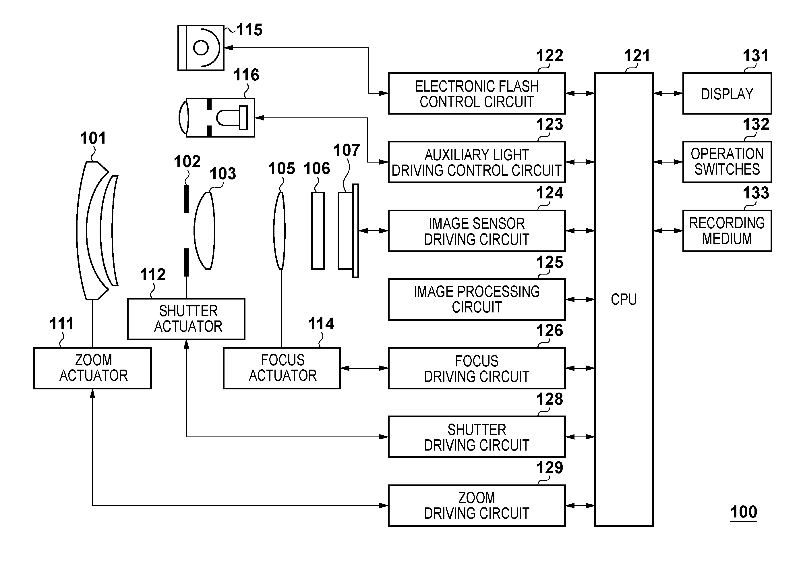
[0029]FIG. 1 is a block diagram illustrating an example of the functional configuration of a digital still camera 100 (to be simply referred to as a camera 100 hereinafter) which exemplifies an image-capturing apparatus using an image sensor according to the first embodiment of the present invention.

[0030]A first lens group 101 is placed at the distal end of an image-capturing optical system (imaging optical system) and held to be movable back and forth along the optical axis. A shutter 102 functions not only as a shutter which controls the exposure time in capturing a still image, but also as an aperture stop which adjusts the opening size to adjust the amount of light in capturing an image. A second lens group 103 placed on the back side (image sensor side) of the shutter 102 can move back and forth along the optical axis together with the shutter 102, and implements a zoom function together with the first lens group 101.

[0031]A third lens group 105 serves as focus lenses and can ...

second embodiment

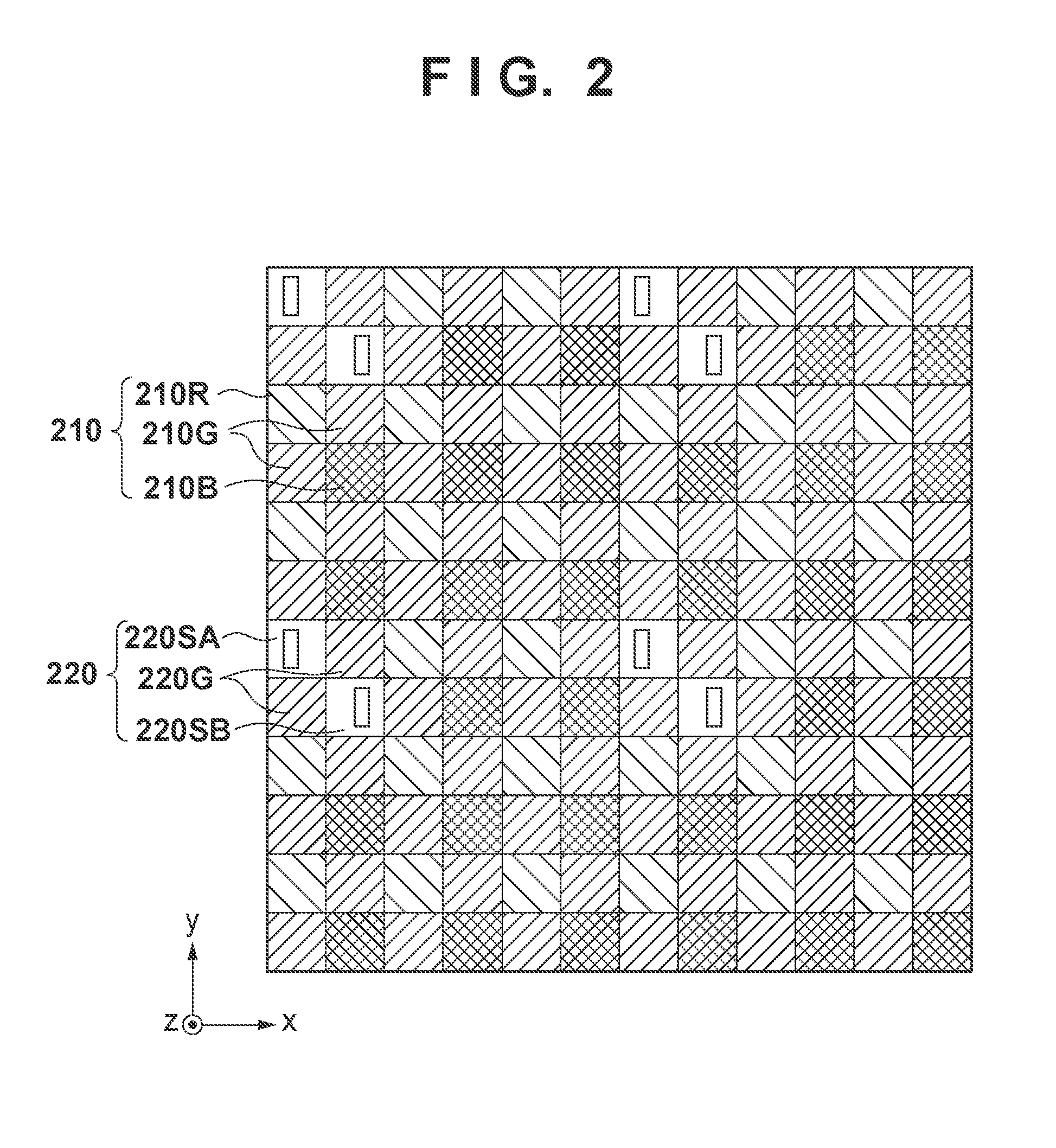
[0085]In the first embodiment, G filters are formed in the focusing pixels 220SA and 220SB shown in FIG. 2, as in the imaging pixel 220G. In contrast to this, in the second embodiment, focusing pixels 220SA and 220SB serve as W (White) pixels, instead of forming color filters in them.

[0086]FIG. 13A is a plan view of the focusing pixel 220SA of the second embodiment when viewed from the side of the light-receiving surface of an image sensor 107 (+z side), and FIG. 13B is a sectional view taken along a cross-section a-a in FIG. 13A when viewed from the −y side. Because no color filter is formed in the focusing pixel 220SA in this embodiment, light-reception efficiency can be improved. Note that the focusing pixel 220SB has the same structure as the focusing pixel 220SA except that a light-shielding layer 310b in the former has an opening position different from a light-shielding layer 310a in the latter.

[0087]In this embodiment, a G filter is formed in an imaging pixel 220G, while no ...

third embodiment

[0091]FIG. 14 is a schematic circuit diagram of an imaging pixel 220G according to the third embodiment. The same reference numerals as in FIG. 6 denote the same constituent elements in FIG. 14, and a repetitive description thereof will not be given. The imaging pixel 220G according to this embodiment has a feature in that an n-type charge-accumulating layer 303 is connected to an additional n-type charge-accumulating layer 307 via a capacitance adjusting gate 308.

[0092]Hence, an effective charge-accumulating layer of a source follower circuit in this embodiment is formed by combining the n-type charge-accumulating layer 303 and the additional n-type charge-accumulating layer (additional charge-accumulating layer) 307. When a capacitance adjusting gate voltage φF is turned off, only the n-type charge-accumulating layer 303 is enabled, so the combined capacitance of all the charge-accumulating layers decreases. On the other hand, when the capacitance adjusting gate voltage φF is turn...


PUM


Abstract

The capacitance of a charge-accumulating layer of an imaging pixel is made different from that of a charge-accumulating layer of a focusing pixel, thereby reducing the difference in saturation capacitance due to the difference between the light-reception efficiencies of the imaging pixel and the focusing pixel. The ratio between the capacitance of the charge-accumulating layer of the imaging pixel and that of the charge-accumulating layer of the focusing pixel is determined in consideration of a variation in ratio between the light-reception efficiencies of the imaging pixel and the focusing pixel with a change in at least one of the exit pupil distance and the aperture value.

Description

BACKGROUND OF THE INVENTION[0001]1. Field of the Invention[0002]The present invention relates to an image sensor and an image-capturing apparatus.[0003]2. Description of the Related Art[0004]There has been proposed an image-capturing apparatus which performs focus detection of an imaging lens by the phase-difference detection method using a two-dimensional image sensor including pixels each having a microlens formed in it.[0005]Japanese patent Laid-Open No. 2000-156823 discloses an image-capturing apparatus including a plurality of pairs of focusing pixels arranged on a two-dimensional image sensor including a plurality of pixels. One pair of focusing pixels are configured to receive light fluxes from different areas in the exit pupil of the imaging lens using a light-shielding layer including an opening, thereby performing pupil division. Imaging signals are obtained by imaging pixels arranged in most parts of the two-dimensional image sensor, and a defocus amount is obtained based...

Claims


Application Information

Patent Timeline
Patent Type & Authority Applications(United States)
IPC IPC(8): H04N5/335H04N5/232
CPCH01L27/14605H01L27/1461H01L27/14623H04N9/045H04N5/2256H04N5/232H04N5/3696H01L27/1463H01L27/14621H01L27/14627H04N23/56H04N23/672H04N25/704H04N23/10
Inventor FUKUDA, KOICHI
Owner CANON KK
Why Eureka
Try Eureka