Stacked Composite Device Including a Group III-V Transistor and a Group IV Lateral Transistor

a composite device and group iii-v technology, applied in the field of group iiinitride and group iv composite devices, can solve the problems of increasing the thermal dissipation requirements of the package, affecting the performance of the device,

Active Publication Date: 2012-10-11
INFINEON TECH AMERICAS CORP
View PDF6 Cites 42 Cited by
  • Summary
  • Abstract
  • Description
  • Claims
  • Application Information

AI Technical Summary

Problems solved by technology

However, conventional packaging techniques for combining HI-Nitride transistors with silicon FETs, for example, often counterweigh the benefits provided by III-Nitride devices.
Such side-by-side configuration can undesirably increase the parasitic inductance and resistance in the current paths of the composite power device, and would also increase the thermal dissipation requirements of the package.
Moreover, the side-by-side placement of devices on a common substrate can undesirably increase package form factor, as well as manufacturing costs.

Method used


Image

  • Stacked Composite Device Including a Group III-V Transistor and a Group IV Lateral Transistor
  • Stacked Composite Device Including a Group III-V Transistor and a Group IV Lateral Transistor
  • Stacked Composite Device Including a Group III-V Transistor and a Group IV Lateral Transistor

Examples


Embodiment Construction

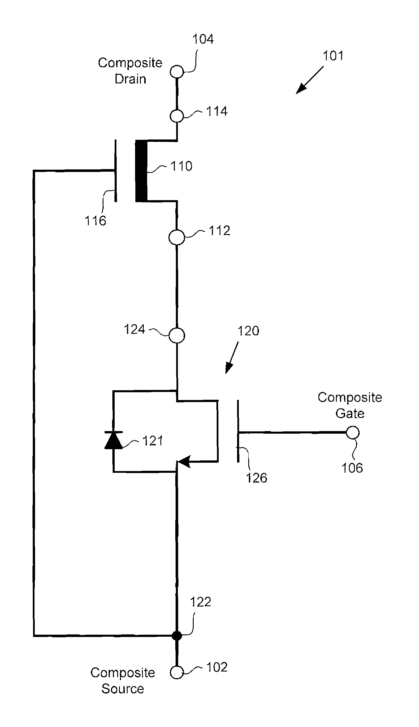
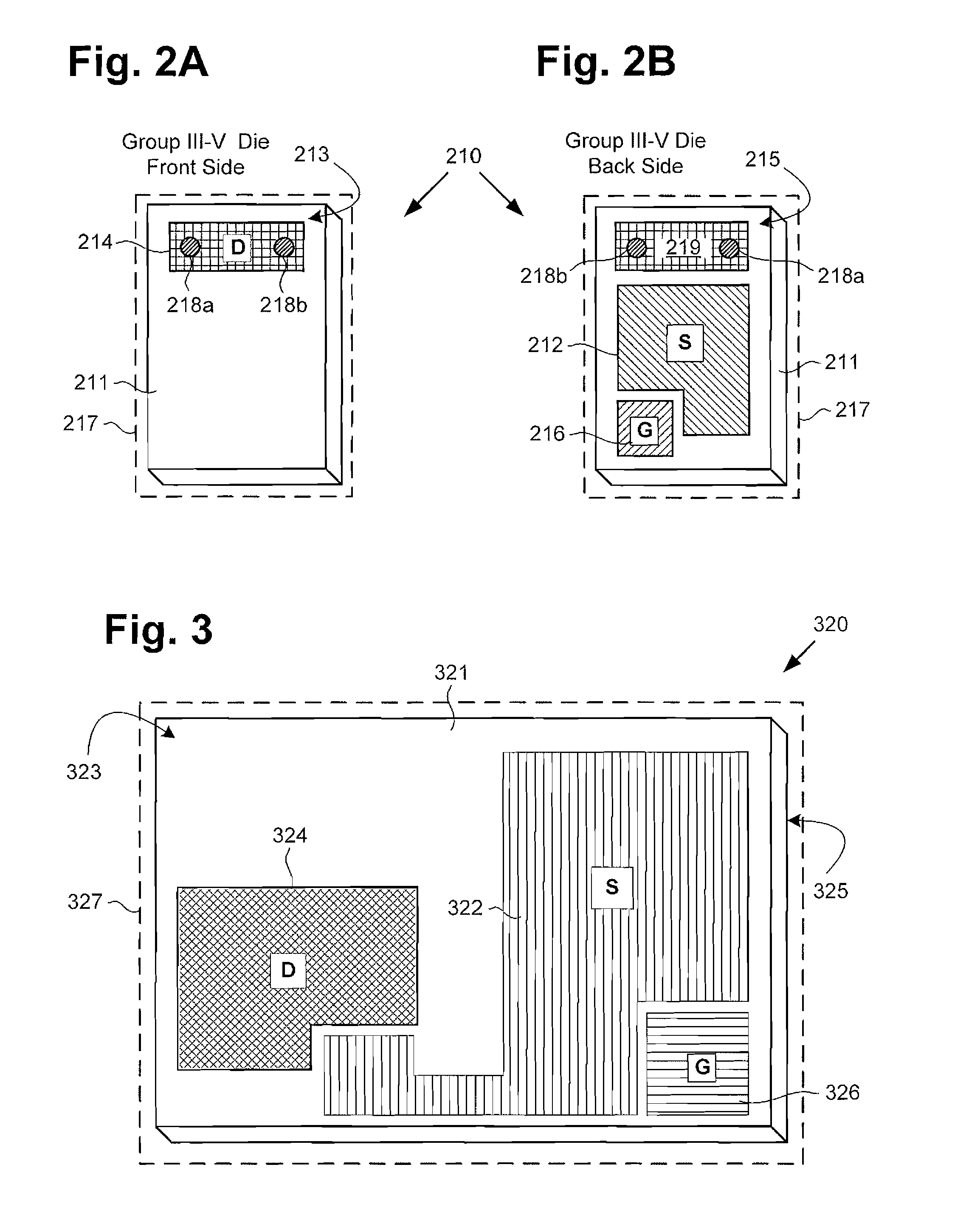
[0018]The following description contains specific information pertaining to implementations in the present disclosure. One skilled in the art will recognize that the present disclosure may be implemented in a manner different from that specifically discussed herein. The drawings in the present application and their accompanying detailed description are directed to merely exemplary implementations. Unless noted otherwise, like or corresponding elements among the figures may be indicated by like or corresponding reference numerals. Moreover, the drawings and illustrations in the present application are generally not to scale, and are not intended to correspond to actual relative dimensions.

[0019]III-Nitride materials include, for example, gallium nitride (GaN) and its alloys such as aluminum gallium nitride (AIGaN), indium gallium nitride (InGaN), and aluminum indium gallium nitride (AlInGaN). These materials are semiconductor compounds that have a relatively wide, direct bandgap and ...


PUM


Abstract

In one implementation, a stacked composite device comprises a group IV lateral transistor and a group III-V transistor stacked over the group IV lateral transistor. A drain of the group IV lateral transistor is in contact with a source of the group III-V transistor, a source of the group IV lateral transistor is coupled to a gate of the group III-V transistor to provide a composite source on a top side of the stacked composite device, and a drain of the group III-V transistor provides a composite drain on the top side of the stacked composite device. A gate of the group IV lateral transistor provides a composite gate on the top side of the stacked composite device, and a substrate of the group IV lateral transistor is on a bottom side of the stacked composite device.

Description

BACKGROUND[0001]The present application claims the benefit of and priority to a pending provisional application entitled “Group III-Nitride and Group IV Composite Device,” Ser. No. 61 / 473,907 filed on Apr. 11, 2011. The disclosure in this pending provisional application is hereby incorporated fully by reference into the present application.[0002]I. Definitions[0003]As used herein, the phrase “group III-V” refers to a compound semiconductor including at least one group III element and at least one group V element. By way of example, a group III-V semiconductor may take the form of a III-Nitride semiconductor. “III-Nitride” or “III-N” refers to a compound semiconductor that includes nitrogen and at least one group III element including aluminum (Al), gallium (Ga), indium (In), and boron (B), and including but not limited to any of its alloys, such as aluminum gallium nitride (AlxGa(1−x)N), indium gallium nitride (InyGa(1−y)N), aluminum indium gallium nitride (AlxInyGa(1−x−y)N), galliu...

Claims


Application Information

Patent Timeline
Patent Type & Authority Applications(United States)
IPC IPC(8): H01L29/20H01L27/088
CPCH01L25/074H03K17/567H01L2924/1305H01L2924/30107H01L2924/13055H01L2224/48091H01L2924/13091H01L25/18H01L2924/00014H01L2924/00
Inventor MCDONALD, TIMBRIERE, MICHAEL A.
Owner INFINEON TECH AMERICAS CORP
Why Eureka
Try Eureka