Oxide stress reduction for a cascode stack circuit

a stack circuit and cascode technology, applied in pulse generators, pulse techniques, instruments, etc., can solve the problems of reducing destroying the oxide layer, and affecting the efficiency so as to reduce the oxide stress of the cascode stack and reduce the oxide stress

Active Publication Date: 2014-10-14
NVIDIA CORP
View PDF5 Cites 18 Cited by
  • Summary
  • Abstract
  • Description
  • Claims
  • Application Information

AI Technical Summary

Benefits of technology

[0003]Embodiments of the present disclosure provide a reduced oxide stress cascode stack circuit and a method of reducing oxide stress in a cascode stack circuit.

Problems solved by technology

As semiconductor device dimensions are reduced, thickness of the oxide layer is also reduced thereby causing the oxide layer to become more vulnerable to gate-to-source and drain-to-source voltages.
If these voltages become too great, oxide breakdown occurs resulting in the destruction of the oxide layer.
In extreme cases, this breakdown may take the form of oxide rupture or oxide punch-through causing spurious current flows and heat generation that further lead to failure of the semiconductor device.
More subtle degradation of the oxide layer also may occur leading to oxide degradation and failure over time.
Circuits designed to provide higher voltage signaling while employing lower voltage devices are particularly sensitive to oxide degradation issues.

Method used


Image

  • Oxide stress reduction for a cascode stack circuit
  • Oxide stress reduction for a cascode stack circuit
  • Oxide stress reduction for a cascode stack circuit

Examples


Embodiment Construction

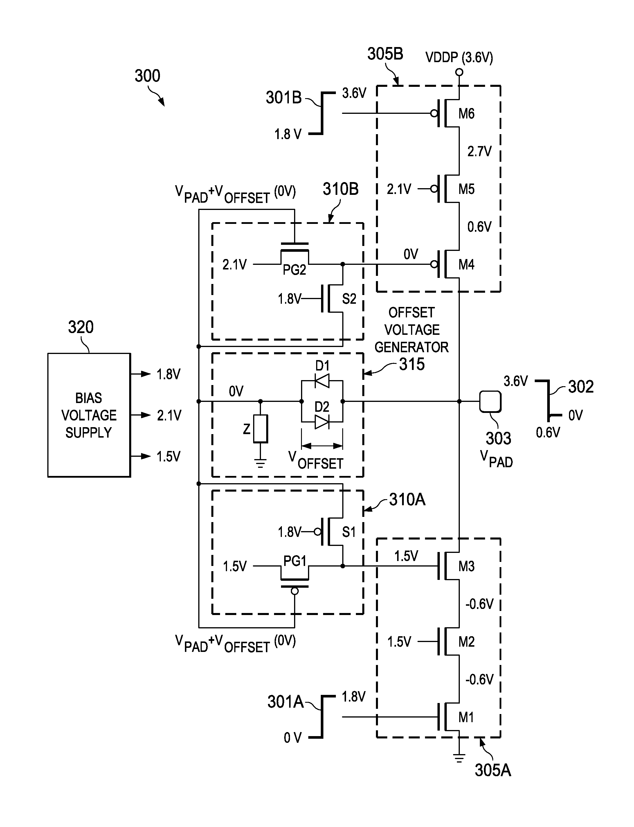
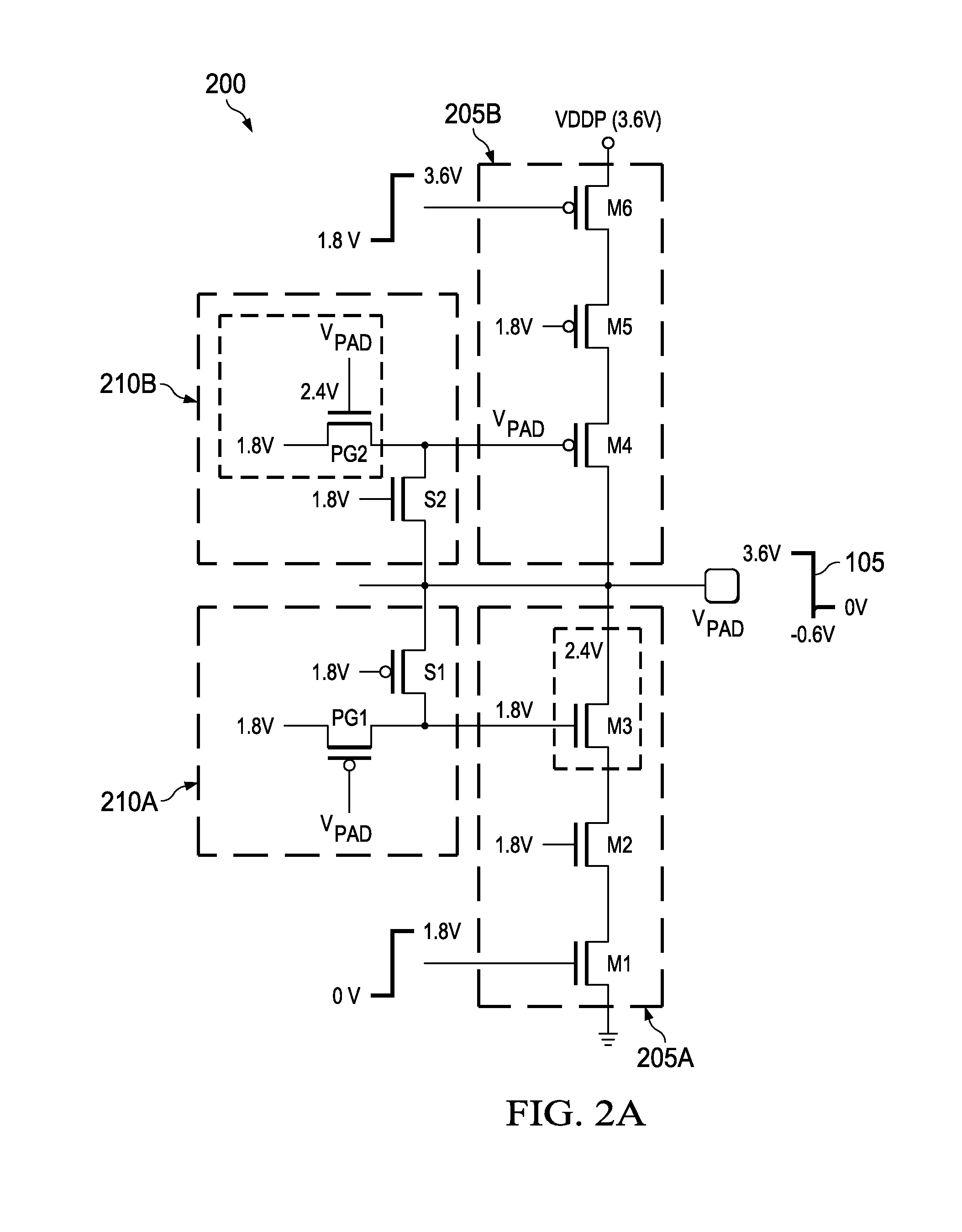
[0012]Embodiments of the present disclosure reduce transient voltage oxide degradation conditions of component transistors employed in cascode stack circuits, wherein steady-state output voltage signaling exceeds component transistor oxide reliability voltage values. Protection is provided for both transient voltage overshoot and undershoot conditions. In this disclosure, oxide reliability voltage is defined as a voltage that provides an oxide stress corresponding to an oxide remaining adequately functional over a long period of time. Here, embodiments of the present disclosure allow tailoring of this period of time to meet a particular requirement or constraint.

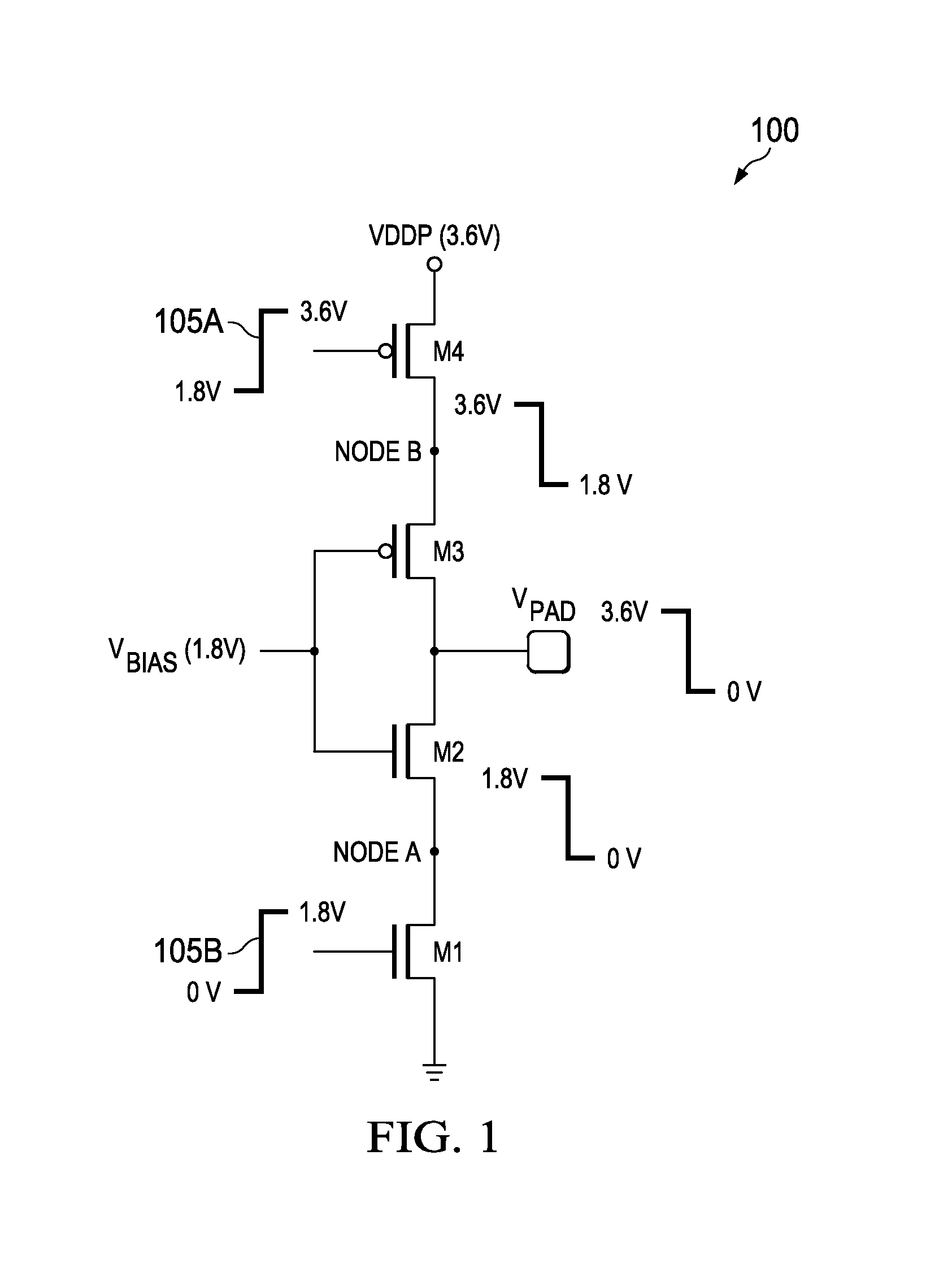
[0013]FIG. 1 illustrates a schematic diagram of a cascode transistor stack, generally designated 100, that provides output signal amplitudes greater than an oxide reliability voltage of its component transistors. The cascode transistor stack 100 illustrates a cascode structure and includes a pair of NMOS transistors M1, M2 a...


PUM


Abstract

A reduced oxide stress cascode stack circuit includes a cascade transistor stack and dynamic bias circuits that supply an output voltage having a magnitude greater than an oxide reliability voltage of their component transistors. The reduced oxide stress cascode stack circuit also includes an offset voltage generator that provides an offset voltage based on a transient extreme of the output voltage, wherein the offset voltage is applied to the cascade transistor stack and the dynamic bias circuits to reduce component transistor voltages commensurate with the oxide reliability voltage. The reduced oxide stress cascode stack circuit further includes a bias voltage supply that modifies a bias voltage value of the cascade transistor stack and dynamic bias circuits by an amount proportional to the offset voltage. A method of reducing oxide stress in a cascode stack circuit is also provided.

Description

TECHNICAL FIELD[0001]This application is directed, in general, to an integrated circuit and, more specifically, to a reduced oxide stress cascode stack circuit and a method of reducing oxide stress in a cascode stack circuit.BACKGROUND[0002]Oxide layers are used in many parts of a semiconductor device such as the dielectric layer in capacitors, the gate oxide between the metal and the semiconductor in MOS transistors and the inter-layer dielectric to isolate conductors from each other, for example. As semiconductor device dimensions are reduced, thickness of the oxide layer is also reduced thereby causing the oxide layer to become more vulnerable to gate-to-source and drain-to-source voltages. If these voltages become too great, oxide breakdown occurs resulting in the destruction of the oxide layer. In extreme cases, this breakdown may take the form of oxide rupture or oxide punch-through causing spurious current flows and heat generation that further lead to failure of the semicond...

Claims


Application Information

Patent Timeline
Patent Type & Authority Patents(United States)
IPC IPC(8): G05F1/10H02M3/04
CPCH02M3/04H03K17/0822
Inventor PATTNAYAK, TAPANYU, SHIFENG
Owner NVIDIA CORP
Why Eureka
Try Eureka