
Stacked NMOS DC-to-DC power conversion

a technology of stacked nmos and dc, applied in the field of power conversion, can solve the problems of linear regulators that linear regulators are very inefficient in many applications, and the linear regulator can only reduce and not increase voltag

Active Publication Date: 2012-07-03
R2 SEMICON
View PDF25 Cites 18 Cited by
  • Summary
  • Abstract
  • Description
  • Claims
  • Application Information

AI Technical Summary

Problems solved by technology

However, they have two important limitations.
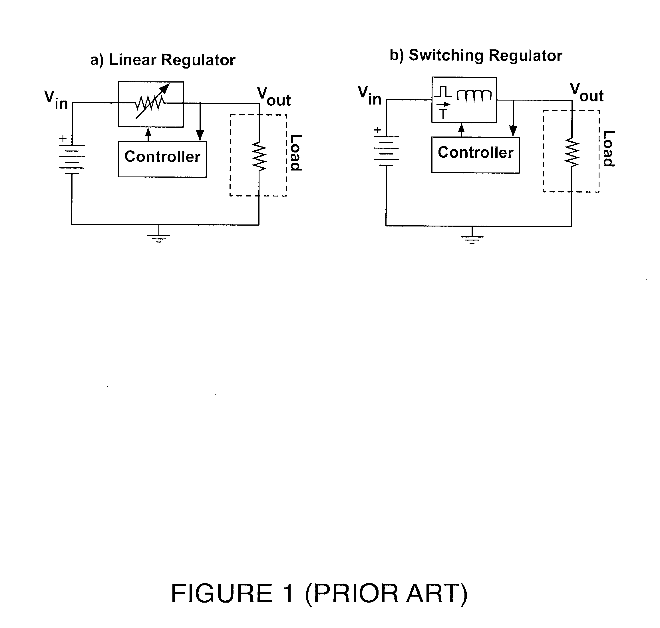
First, a linear regulator can only reduce and not increase the voltage presented to it.
Secondly, linear regulators are very inefficient in many applications (or in cases where the output voltage is not slightly below the input voltage).
Thus, when a substantial reduction in the input voltage is called for by the application, a linear regulator must inevitably provide poor efficiency.
Particularly in the case of battery-powered devices, inefficient voltage regulation directly impacts the expected battery life and thus is highly undesirable.
Unfortunately, most switched mode regulators require large valued (and physically large and thick) external inductors and capacitors to operate.
), and limitations on the peak current due to core saturation effects.
Core saturation leads to a significant reduction in inductance and an increase in loss, (both of the latter due to a large increase in inductor current).
Therefore, the inductor cannot be allowed to saturate during normal regulator operation.
Switching frequency can be increased to reduce the peak current encountered, but as noted above, at high frequencies the saturation magnetization falls, setting a limit on how much improvement can be obtained in that manner.
At higher frequency the core losses begin to increase rapidly and efficiency falls.
Wound magnetic inductors are bulky compared to components integrated on a semiconductor chip.
For battery-operated devices, the height of the electronic components mounted in the internal printed circuit board (PCB) is usually limited by the thickness of the inductors used for DC-DC power conversion.
For converters operating at 10 MHz or less, the capacitor is typically 5 μF or larger, again adding substantially to the size and expense of the converter.
While magnetic materials may still be employed, their deposition requires additional process steps and thus adds cost.
However, during the time Tsw when the transistor transitions from the open to closed state, or vice versa, large voltages and currents may be simultaneously present, and losses can be substantial due to power being dissipated across the switching devices.
Secondly, the voltage on the gate of a transistor must be changed in order to switch its state from open to closed or closed to open.
The node capacitance may intrinsically be very small, causing rapid changes in voltage and making it difficult to maintain correct switch timing, so it is typical to add capacitance to the node or in parallel with the switching transistors, depicted in FIG. 7 as Cseries and Cshunt, to simplify the problem of accurate switch timing.
However, such circuitry operates optimally only over a narrow band of frequencies and presents substantially sinusoidal voltages to the constituent components, so pulse-width modulation (PWM) cannot generally be used to control the output voltage, and other means such as frequency variation or on-off control must be substituted.
Finally, the use of a resonant input may lead to large voltage swings on the switching transistor gates in order to ensure fast switching transients, which can cause reliability problems.
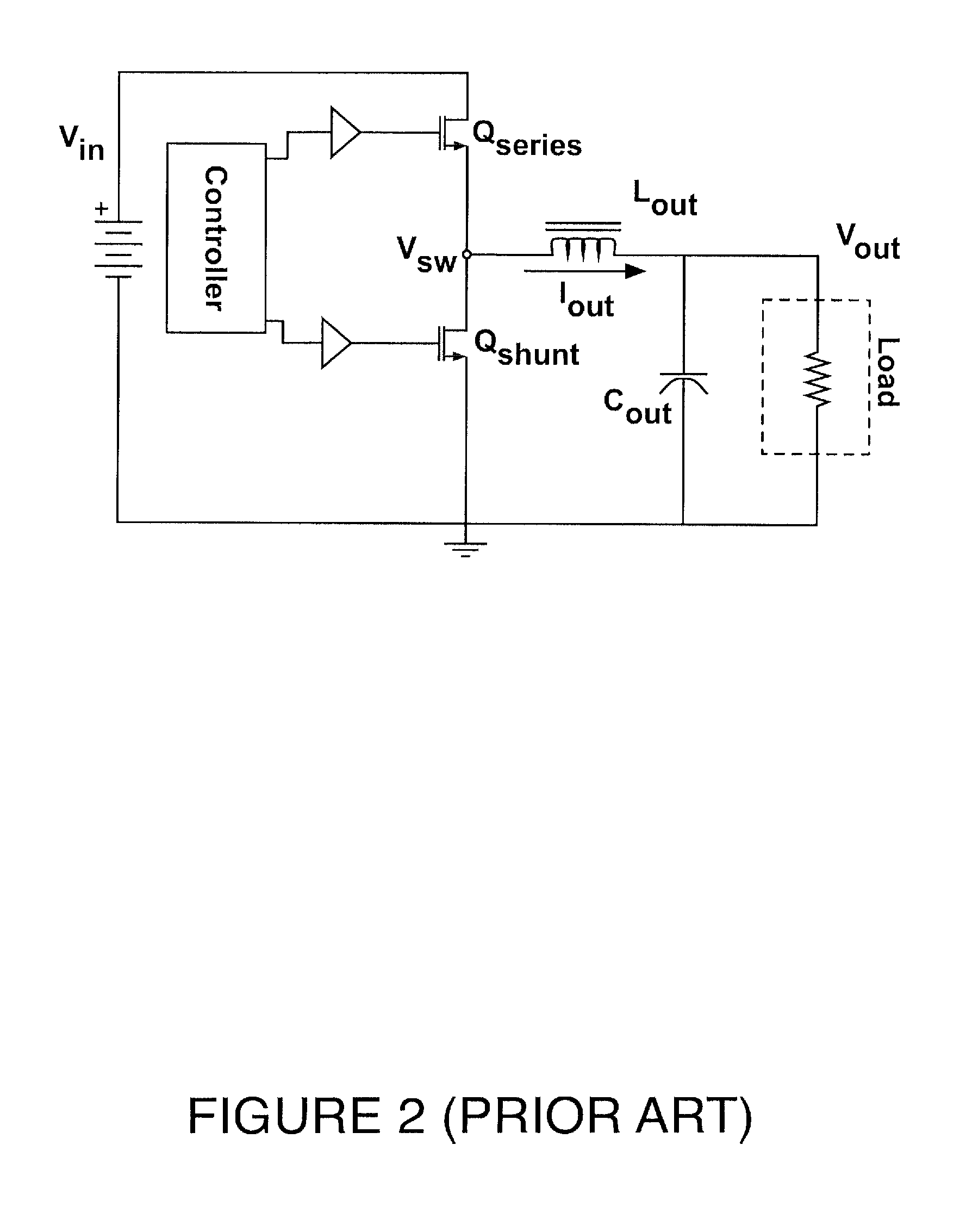
Under these conditions, a conventional buck converter circuit as depicted in FIG. 2 cannot operate reliably.

Method used


Image

  • Stacked NMOS DC-to-DC power conversion
  • Stacked NMOS DC-to-DC power conversion
  • Stacked NMOS DC-to-DC power conversion

Examples


Embodiment Construction

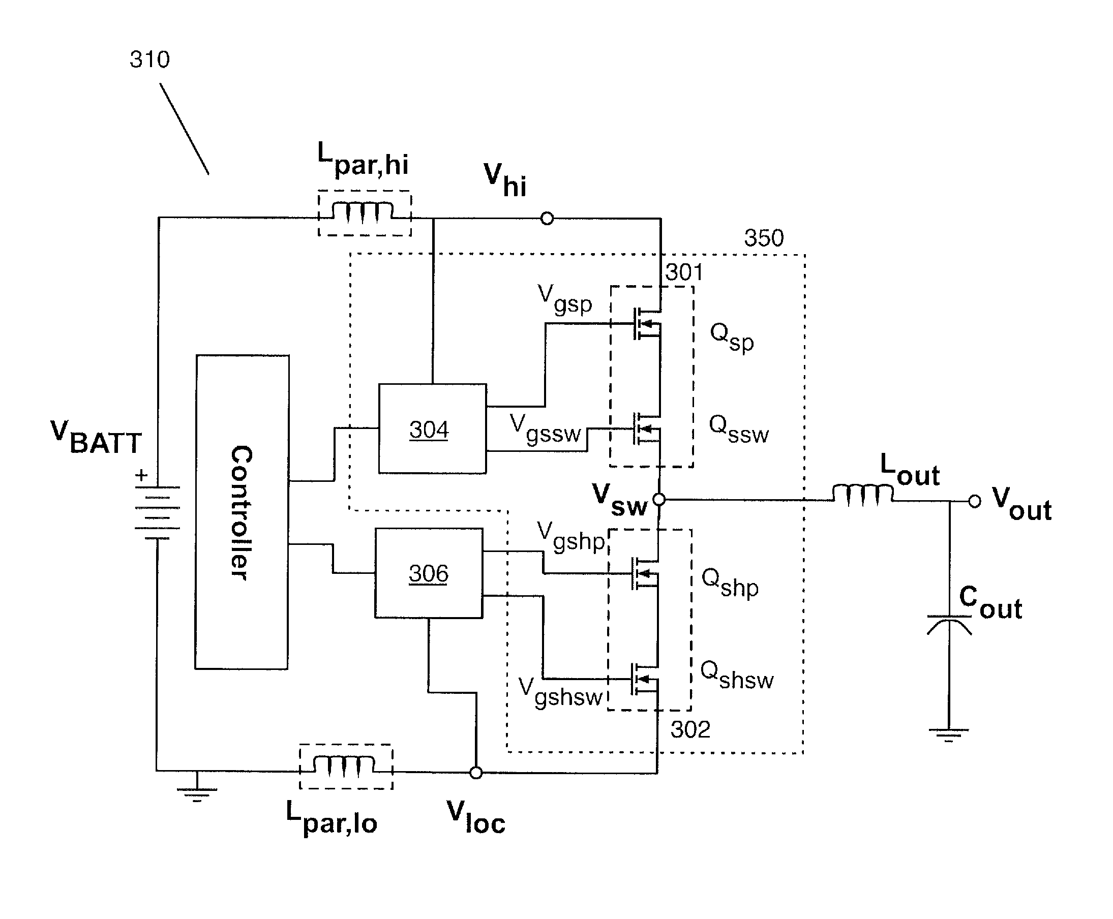
[0001]The described embodiments relate generally to power conversion. More particularly, the described embodiments relate to a stacked NMOS DC-to-DC power conversion.

BACKGROUND

[0002]DC voltage converters and regulators are well-known in the art and are widely employed to ensure that the DC voltage provided to electronic devices is of the correct value independent of variations in the available supply voltage or the load presented by the device being powered. For example, most battery-operated consumer electronics devices use DC-DC regulators to convert the 2.7-5.5 V battery voltage down to a 0.56-3.4 V operating voltage required by the on-board integrated circuits. Voltage regulators are universally used to convert the battery voltage to the desired fixed value to be supplied to the integrated circuit, and to ensure that value remains constant as the battery ages and the current used by the integrated circuit changes.

[0003]Voltage regulators can be classified as either linear mode o...


PUM


Abstract

Embodiments for at least one method and apparatus of generating a regulated voltage are disclosed. One method includes generating the regulated voltage though controlled closing and opening of a series switch element and shunt switch element, the series switch element being connected between a first voltage supply and a common node, and the shunt switch being connected between the common node and a second supply voltage. The series switch element includes an NMOS series switching transistor stacked with an NMOS series protection transistor, and closing the series switch element during a first period includes applying a switching gate voltage to a gate of the NMOS series switch transistor of the series switch element, wherein the switching gate voltage has a voltage potential of at least a threshold voltage greater than a voltage potential of the common node. The shunt switch element includes an NMOS shunt switching transistor stacked with an NMOS shunt protection transistor, and the shunt switch element is closed during a second period.

Description

FIELD OF THE DESCRIBED EMBODIMENTS[0001]The described embodiments relate generally to power conversion. More particularly, the described embodiments relate to a stacked NMOS DC-to-DC power conversion.BACKGROUND[0002]DC voltage converters and regulators are well-known in the art and are widely employed to ensure that the DC voltage provided to electronic devices is of the correct value independent of variations in the available supply voltage or the load presented by the device being powered. For example, most battery-operated consumer electronics devices use DC-DC regulators to convert the 2.7-5.5 V battery voltage down to a 0.56-3.4 V operating voltage required by the on-board integrated circuits. Voltage regulators are universally used to convert the battery voltage to the desired fixed value to be supplied to the integrated circuit, and to ensure that value remains constant as the battery ages and the current used by the integrated circuit changes.[0003]Voltage regulators can be ...

Claims


Application Information

Patent Timeline
IPC IPC(8): G05F1/613
CPCH02M3/156H03K17/102H03K17/122H03K2217/0081H02M1/088H02M3/158
Inventor BURNS, LAWRENCE M.FISHER, DAVID
Owner R2 SEMICON
Learn More