Display device and method for manufacturing the same

a technology of display device and manufacturing method, which is applied in the manufacture of electric discharge tubes/lamps, basic electric elements, instruments, etc., can solve the problems of affecting the display performance of display device, and achieve the effect of preventing unexpected color light leakage, expanding the area of sub-pixel electrodes, and increasing the aperture ratio of sub-pixels

Active Publication Date: 2012-10-11
HIMAX DISPLAY INC
View PDF5 Cites 8 Cited by
  • Summary
  • Abstract
  • Description
  • Claims
  • Application Information

AI Technical Summary

Benefits of technology

[0017]To sum up, it is not necessary to reduce the area of the sub-pixel electrodes according to the embodiments of the invention. In other words, the area of the sub-pixel electrodes can be expanded as much as possible, and the aperture ratio of the sub-pixels can be increased. Each of the color areas of the color filter layer is partially overlapped with two of the sub-pixel electrodes adjacent to each other. Therefore, notwithstanding the FFE on the sub-pixels, the unexpected color light leakage can be prevented to a great extent according to the embodiments of the invention. Accordingly, based on the above embodiments, the issue of FFE can be resolved, and color saturation can be improved.

Problems solved by technology

Apparently, the FFE on the sub-pixels leads to unexpected color light leakage, which is detrimental to the display performance of the display device 100.

Method used


Image

  • Display device and method for manufacturing the same
  • Display device and method for manufacturing the same
  • Display device and method for manufacturing the same

Examples


Embodiment Construction

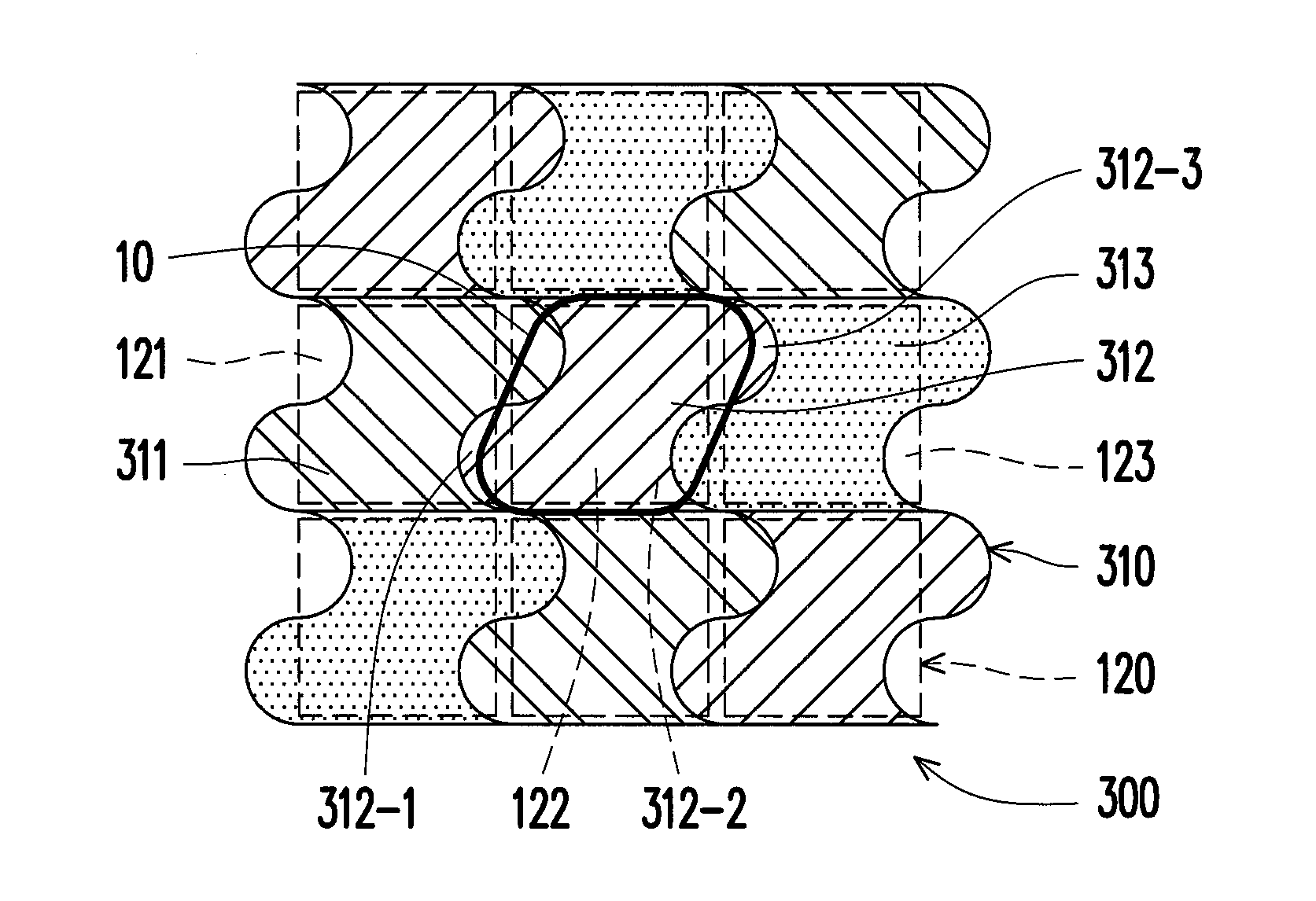
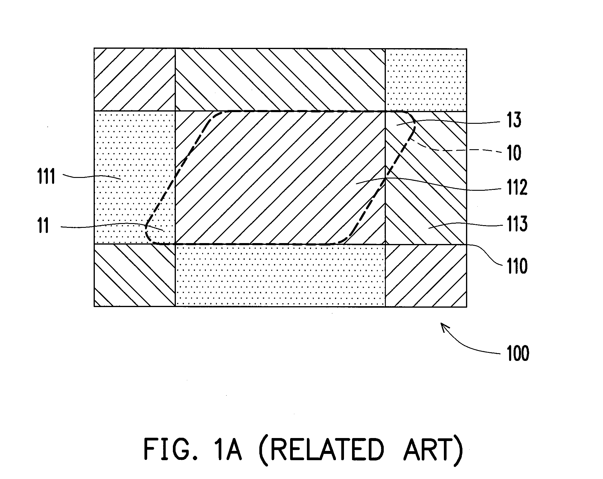
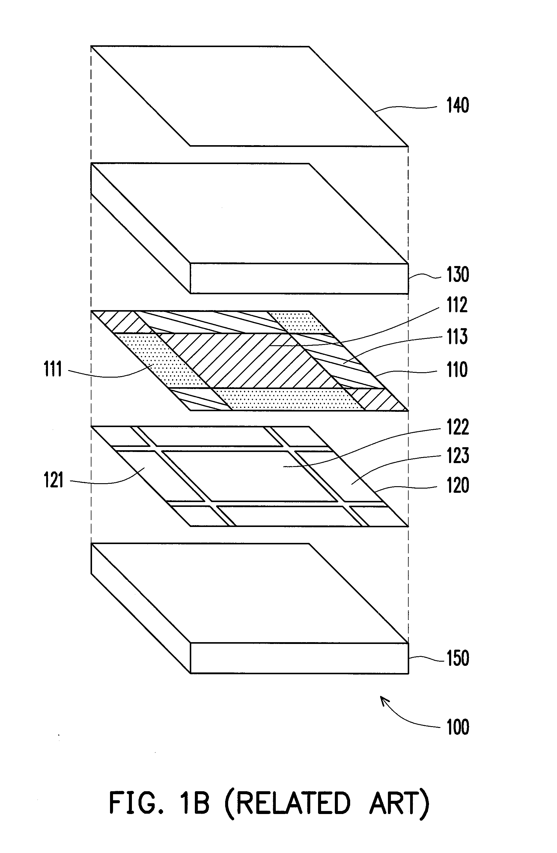
[0034]FIG. 3A is a schematic partial top view illustrating a sub-pixel array of a display device 300 according to an embodiment of the invention. FIG. 3B is a schematic partial top view illustrating the sub-pixel electrode layer 120 depicted in FIG. 3A. FIG. 3C is a schematic partial top view illustrating the color filter layer 310 depicted in FIG. 3A. The display device 300 can be a liquid crystal on silicon (LCOS) display device or any other display panel that has the color filter layer. The descriptions of the sub-pixel electrode layer 120 and other components of the display device 300 in FIG. 3A can be referred to as the descriptions of the display device 100 in FIG. 1. The difference between the display devices 100 and 300 lies in the color filter layer 310 of the display device 300. Specifically, the display device 300 includes a substrate and the color filter layer 310. A plurality of sub-pixel electrodes (e.g., sub-pixel electrodes 121, 122, and 123) of the sub-pixel electro...


PUM

PropertyMeasurementUnit
coloraaaaaaaaaa
shapeaaaaaaaaaa
color areasaaaaaaaaaa

Abstract

A display device and a method for manufacturing the display device are provided. The display device includes a substrate and a color filter layer. A plurality of sub-pixel electrodes are formed on the substrate. The color filter layer is configured on the substrate. The color filter layer defines a plurality of color areas corresponding to the sub-pixel electrodes. Here, each of the color areas is partially overlapped with two of the sub-pixel electrodes adjacent to each other.

Description

CROSS-REFERENCE TO RELATED APPLICATION[0001]This application claims the priority benefit of U.S. Provisional Application Ser. No. 61 / 472,621, filed Apr. 6, 2011. The entirety of the above-mentioned patent application is hereby incorporated by reference herein and made a part of this specification.BACKGROUND OF THE INVENTION[0002]1. Field of the Invention[0003]The invention relates to a display device. More particularly, the invention relates to a display device having a color filter layer and a method for manufacturing the display device.[0004]2. Description of Related Art[0005]The performance of a display device is often subject to a fringe field effect (FFE). Specifically, when the density of sub-pixels is high, or the distance between two adjacent sub-pixels is close, the FFE needs to be taken into consideration. In an exemplary liquid crystal on silicon (LCOS) display device, the density of the sub-pixels is high, and the distance between the adjacent sub-pixels is short. Hence,...

Claims


Application Information

Patent Timeline
Patent Type & Authority Applications(United States)
IPC IPC(8): G02F1/1335H01J9/24
CPCG02F2201/52G02F2001/136222G02F1/133514G02F1/136277G02F1/136222
Inventor LI, YUET-WINGWANG, CHIEN-TANGFAN-CHIANG, KUAN-HSU
Owner HIMAX DISPLAY INC
Why Eureka
Try Eureka