Display Device

a display device and display device technology, applied in the direction of electrical apparatus construction details, inspection/indentification of circuits, instruments, etc., can solve the problems of not being able to measure the contact resistance of an external circuit such as an fpc, and the difficulty of reducing so as to reduce the width of the substrate, reduce the cost, and reduce the size of the display device

Inactive Publication Date: 2012-10-18
JAPAN DISPLAY INC
View PDF4 Cites 15 Cited by
  • Summary
  • Abstract
  • Description
  • Claims
  • Application Information

AI Technical Summary

Benefits of technology

[0008]Generally, a liquid crystal display device for tablet use or mobile use includes a TFT drive circuit and a driver connecting portion which are mounted on the same substrate in view of a module structure and the cost. Thus, smaller substrate widths have been strongly demanded for liquid crystal display devices. The number of circuit components has been reduced and multilayer substrates have been used to reduce the widths of substrates but a reduction in width is limited.
[0010]Japanese Patent Application Laid-Open Publication No. 2007-52146 describes the terminals that are disposed in the external connection area as terminals for measuring a contact resistance, which eliminates the need for providing dedicated terminals for measurement. This technique is usable for measurement of a contact resistance of the drive circuit provided on the substrate but is not usable for measurement of a contact resistance of an external circuit such as an FPC.
[0011]The present invention increases a wiring area on a substrate and reduces the width of the substrate by improving the configuration of a test terminal for measuring a crimp resistance at a connection of an anisotropic conductive film in a display device, thereby achieving a smaller display device at lower cost.
[0021]According to the aspect of the present invention, test terminals for crimp resistance measurement are disposed at crimp dummy terminal portions. Thus, the wiring area of the test terminals can be used as a mounting area of electronic components, the wiring area can be expanded on the substrate and the width of the substrate can be reduced, thereby achieving a smaller display device at lower cost. Furthermore, the test terminals for crimp resistance measurement are disposed on both ends of a crimp area and are arranged in a line on the printed circuit board, thereby facilitating measurement. Moreover, a crimp resistance can be automatically measured by a prober.

Problems solved by technology

The provision of the test pads leads to difficulty in reducing the width of the substrate.
This technique is usable for measurement of a contact resistance of the drive circuit provided on the substrate but is not usable for measurement of a contact resistance of an external circuit such as an FPC.

Method used


Image

  • Display Device
  • Display Device
  • Display Device

Examples


first embodiment

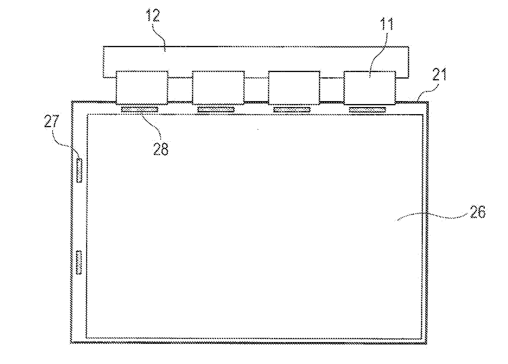
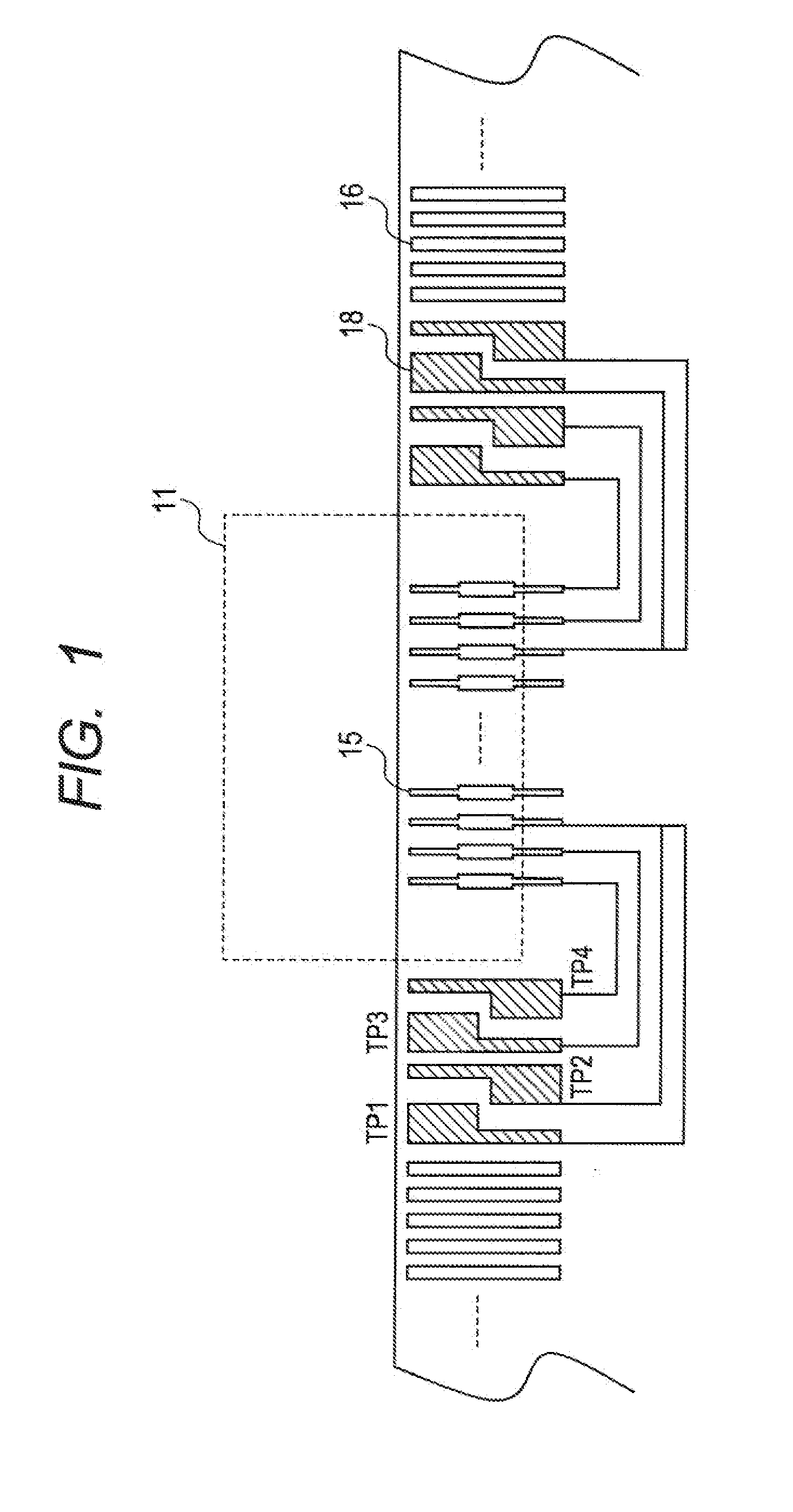
[0047]FIG. 1 illustrates the shapes of crimp contacts and a connection diagram according to the first embodiment of the present invention.

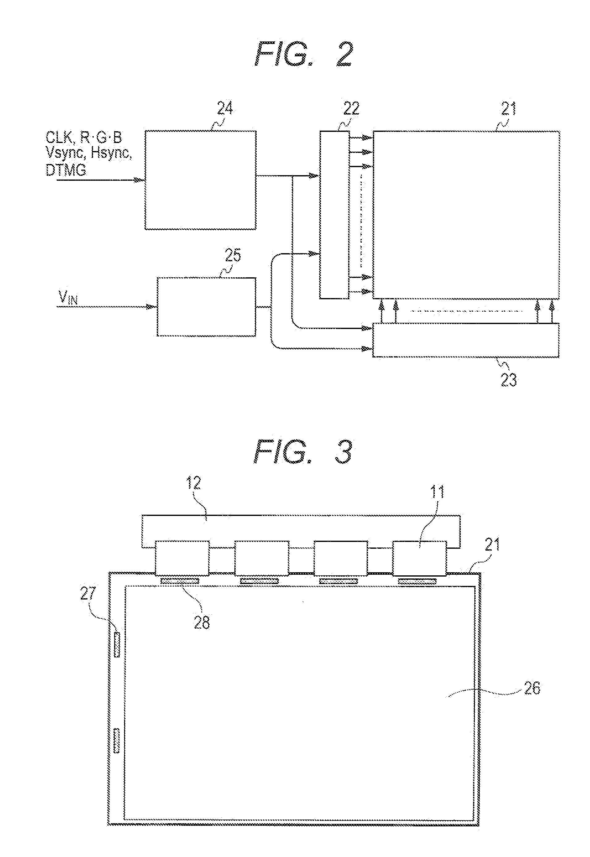
[0048]As in the conventional configuration, a circuit board (e.g., a drain substrate or a gate substrate) includes multiple crimp contacts 15 (first terminals) in the mounting area of an FPC or a COF (that is, an area where the circuit board and the FPC or the COF overlap each other) along one side of the circuit board. The crimp contacts 15 are connected to the FPC or a COF 11 by crimping via an anisotropic conductive film. In non-crimping areas on both sides of the crimp contacts 15, multiple dummy terminals 16 (second terminals) are provided along one side of the substrate.

[0049]Furthermore, test terminals 18 (third terminals) for crimp resistance measurement are disposed on both sides of the crimp contacts 15, that is, at points where the dummy terminals of the conventional configuration are located. Three of the crimp contacts 15 on each side...

second embodiment

[0059]FIG. 6 illustrates the shapes of crimp contacts and a connection diagram according to a second embodiment of the present invention.

[0060]The second embodiment is different from the first embodiment in the shape of a test terminal. In the present embodiment, test terminals 19 are rectangular like dummy terminals 16. The test terminals 19 are distinguished from the dummy terminals 16 by larger intervals than those of the dummy terminals 16. Thus, the test terminals 19 can be identified without being varied in shape from the dummy terminals 16.

third embodiment

[0061]FIG. 7 illustrates the shapes of crimp contacts and a connection diagram according to a third embodiment of the present invention.

[0062]The third embodiment is different from the first embodiment in the positions of test terminals. In the first embodiment, the test terminals 18 are disposed near both sides of the crimp contacts 15, whereas in the third embodiment, test terminals 18 are disposed next to dummy terminals 16 on both sides of crimp contacts 15 and are separated from the crimp contacts 15, facilitating probing more than in the first embodiment.

[0063]The liquid crystal display devices were illustrated in the foregoing embodiments of the present embodiment. The present invention is not limited to a liquid crystal display device and is also applicable to display devices Such as an organic EL display and a plasma display.

[0064]Furthermore, the printed circuit boards (PCB), which are rigid substrates, were illustrated in the embodiments of the present invention. The pres...


PUM


Abstract

A wiring area on a substrate is expanded and the width of the substrate is reduced to achieve a smaller display device at lower cost. The display device includes a display panel, a circuit board, and a flexible printed circuit board connecting the display panel and the circuit board, and the circuit board and the flexible printed circuit board are electrically connected to each other via an anisotropic conductive film. Crimp contacts 15 in the mounting area of the flexible printed circuit board 11 and crimp dummy terminals 16 outside the mounting area are provided on the circuit board, and some of the crimp dummy terminals act as test terminals 18 for crimp resistance measurement, and the crimp contacts 15 and the test terminals 18 are electrically connected to each other on the circuit board.

Description

[0001]The present application claims priority from Japanese patent application JP2011-092378 filed on Apr. 18, 2011, the content of which is hereby incorporated by reference into this application.BACKGROUND OF THE INVENTION[0002]1. Field of the Invention[0003]The present invention relates to display device such as liquid crystal display device and, in particular, to a display device having an improved structure for measuring an electrical connection between a substrate having an electronic device and a flexible printed circuit board.[0004]2. Description of the Related Art[0005]For example, a liquid crystal display device includes a liquid crystal display panel having a pixel area on a substrate, a printed circuit board (PCB) having electronic devices such as an IC, and a flexible printed circuit board (FPC) for electrically connecting the substrate of the liquid crystal display panel and the terminals of the printed circuit board. To reduce the size of the liquid crystal display dev...

Claims


Application Information

Patent Timeline
Patent Type & Authority Applications(United States)
IPC IPC(8): H05K7/00
CPCG02F1/13452H01L27/3297H05K1/0268H05K3/361H05K2201/09781H01L2924/0002H05K2201/10128H01L2924/00H10K59/131
Inventor YAMAGISHI, YASUHIKO
Owner JAPAN DISPLAY INC
Why Eureka
Try Eureka