Organic light emitting diode display

a light-emitting diode and organic technology, applied in the field of organic light-emitting diodes (oled) displays, can solve the problems of reducing stability, reducing durability, and deteriorating quality of organic light-emitting diodes, so as to effectively add an element such as a touch sensor, improve durability and vapor transmission resistance, effect of suppressing external light reflection

Inactive Publication Date: 2012-10-25
SAMSUNG DISPLAY CO LTD
View PDF10 Cites 23 Cited by
  • Summary
  • Abstract
  • Description
  • Claims
  • Application Information

AI Technical Summary

Benefits of technology

[0025]According to an embodiment, the organic light emitting diode (OLED) display improves durability and vapor transmission resistance, efficiently suppresses reflection of external light, and effectively adds an element such as a touch sensor.

Problems solved by technology

Therefore, when the organic emission layer is exposed to moisture and oxygen, the quality of the organic light emitting diode display is deteriorated.
However, the frit is relatively easily damaged by an impact to reduce stability.
Further, when the thin film encapsulation layer is used, vapor transmission resistance of the thin film encapsulation layer may be relatively insufficient at the side of the device.

Method used


Image

  • Organic light emitting diode display
  • Organic light emitting diode display
  • Organic light emitting diode display

Examples


first embodiment

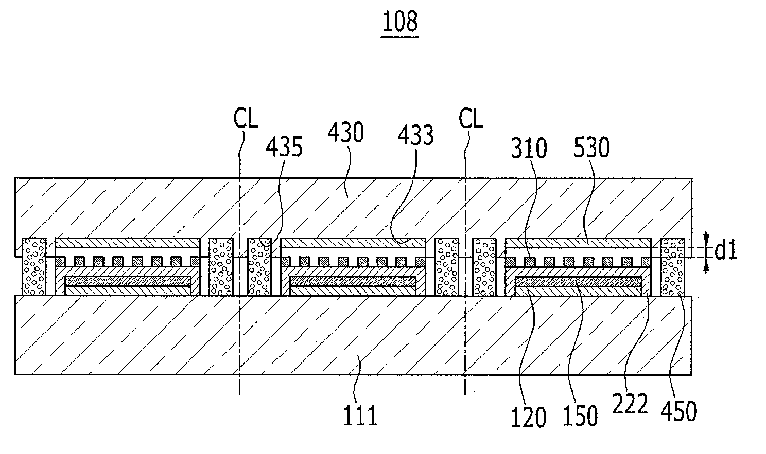
[0038]Referring to FIG. 1, an organic light emitting diode (OLED) display 101 will now be described.

[0039]As shown in FIG. 1, the organic light emitting diode (OLED) display 101 includes a display substrate 111, a driving circuit 120, an organic light emitting element 150, a thin film encapsulation layer 222, a light blocking pattern layer 310, a sealant 450, and an encapsulation member 410.

[0040]The display substrate 111 is formed with a transparent insulation substrate made of glass, quartz, or ceramic.

[0041]The driving circuit 120 is formed on the display substrate 111. The driving circuit 120 includes a plurality of thin film transistors and capacitors and drives the organic light emitting element 150.

[0042]The organic light emitting element 150 is formed on the display substrate 111, and is electrically connected to the driving circuit 120. The organic light emitting element 150 outputs light in response to a driving signal provided by the driving circuit 120. In this instance...

second embodiment

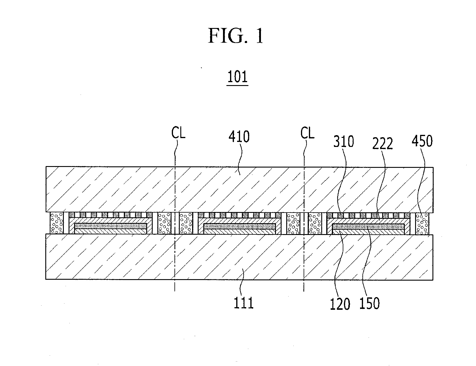
[0057]A second embodiment will now be described with reference to FIG. 2.

[0058]As shown in FIG. 2, the organic light emitting diode (OLED) display 102 according to the second embodiment uses a polarizing member 320 as a member for suppressing reflection of external light.

[0059]The polarizing member 320 includes a plurality of optical films such as a polarizing plate and a phase delay plate, and it can have various types of configurations known to a person skilled in the art. The polarizing member 320 can suppress the reflection of the external light more effectively than the light blocking pattern layer 310 used in the first embodiment.

[0060]In the second embodiment, the polarizing member 320 is protected by using the encapsulation member 410 so that the damage and contamination of the polarizing member 320 can be minimized in an efficient manner.

[0061]By the above-described configuration, the organic light emitting diode (OLED) display 102 according to the second embodiment can eff...

third embodiment

[0062]Referring to FIG. 3, a third embodiment will now be described.

[0063]As shown in FIG. 3, the organic light emitting diode (OLED) display 103 according to the third embodiment uses a film made of a resin material for the encapsulation member 420. For example, the encapsulation member 420 can be a polyimide (PI) film with excellent heat resistance, chemical resistance, and insulation.

[0064]The thin film encapsulation layer 222 is formed in the space that is sealed by the sealant 450 and the encapsulation member 420. Thus, the encapsulation member 420 can be made with a resin-based film even though it has lower vapor transmission resistance than a glass substrate. That is, the encapsulation member 420 can be formed with polyimide that is relatively easy to use in manufacture and that is inexpensive. Also, when the resin-type film is used for the encapsulation member 420, the thickness of the organic light emitting diode (OLED) display 103 can be reduced.

[0065]Further, the bonding ...


PUM


Abstract

An organic light emitting diode (OLED) display includes: a display substrate; an organic light emitting element formed over the display substrate; a thin film encapsulation layer formed over the display substrate to cover the organic light emitting element; an encapsulation member facing the display substrate with the organic light emitting element and the thin film encapsulation layer therebetween; a sealant surrounding the organic light emitting element and the thin film encapsulation layer disposed between the display substrate and the encapsulation member, and bonding the display substrate and the encapsulation member; and a light control member disposed between the encapsulation member and the thin film encapsulation layer.

Description

RELATED APPLICATIONS[0001]This application claims priority to and the benefit of Korean Patent Application No. 10-2011-0037379 filed in the Korean Intellectual Property Office on Apr. 21, 2011, the entire contents of which are incorporated herein by reference.BACKGROUND[0002]1. Field[0003]The present disclosure relates generally to an organic light emitting diode (OLED) display. More particularly, the present disclosure relates to an organic light emitting diode (OLED) display for improving an encapsulation configuration.[0004]2. Description of the Related Art[0005]OLED displays are flat panel displays that can be made lightweight and thin because they have self-luminous characteristics and require no separate light source. Particularly, since the OLED displays exhibit high quality characteristics such as low power consumption, high luminance, high response speed, and thus, the OLED displays receives much attention as next-generation display devices.[0006]An OLED display includes a ...

Claims


Application Information

Patent Timeline
Patent Type & Authority Applications(United States)
IPC IPC(8): H01L51/52H01L51/56
CPCH01L51/524H01L27/323H01L51/5281H10K59/40H10K50/841H10K50/86H05B33/04H10K50/8426H10K50/84
Inventor HAN, BYUNG-UKYOO, EUI-JINKIM, JAE-YONGJEONG, CHUL-WOOKIM, SEON-HEECHAE, BYUNG-HOONKIM, GUN-MO
Owner SAMSUNG DISPLAY CO LTD
Why Eureka
Try Eureka