Semiconductor device

a technology of semiconductor devices and devices, applied in semiconductor devices, semiconductor/solid-state device details, electrical equipment, etc., can solve problems such as air bridges being crushed

Active Publication Date: 2012-10-25
SUMITOMO ELECTRIC DEVICE INNOVATIONS
View PDF7 Cites 35 Cited by
  • Summary
  • Abstract
  • Description
  • Claims
  • Application Information

AI Technical Summary

Problems solved by technology

However, the structure disclosed in Document 1 fails to realize a strong mechanical strength of the air bridges, and has a possibility that the air bridges may be crushed due to external force applied thereto.

Method used


Image

  • Semiconductor device
  • Semiconductor device
  • Semiconductor device

Examples


first embodiment

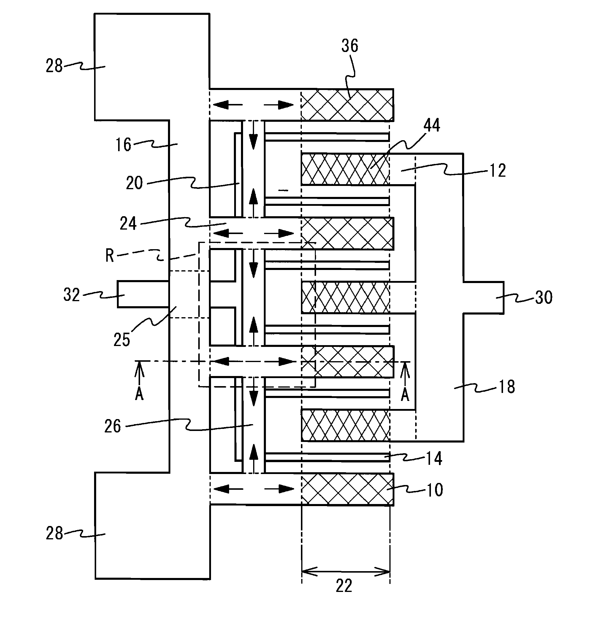
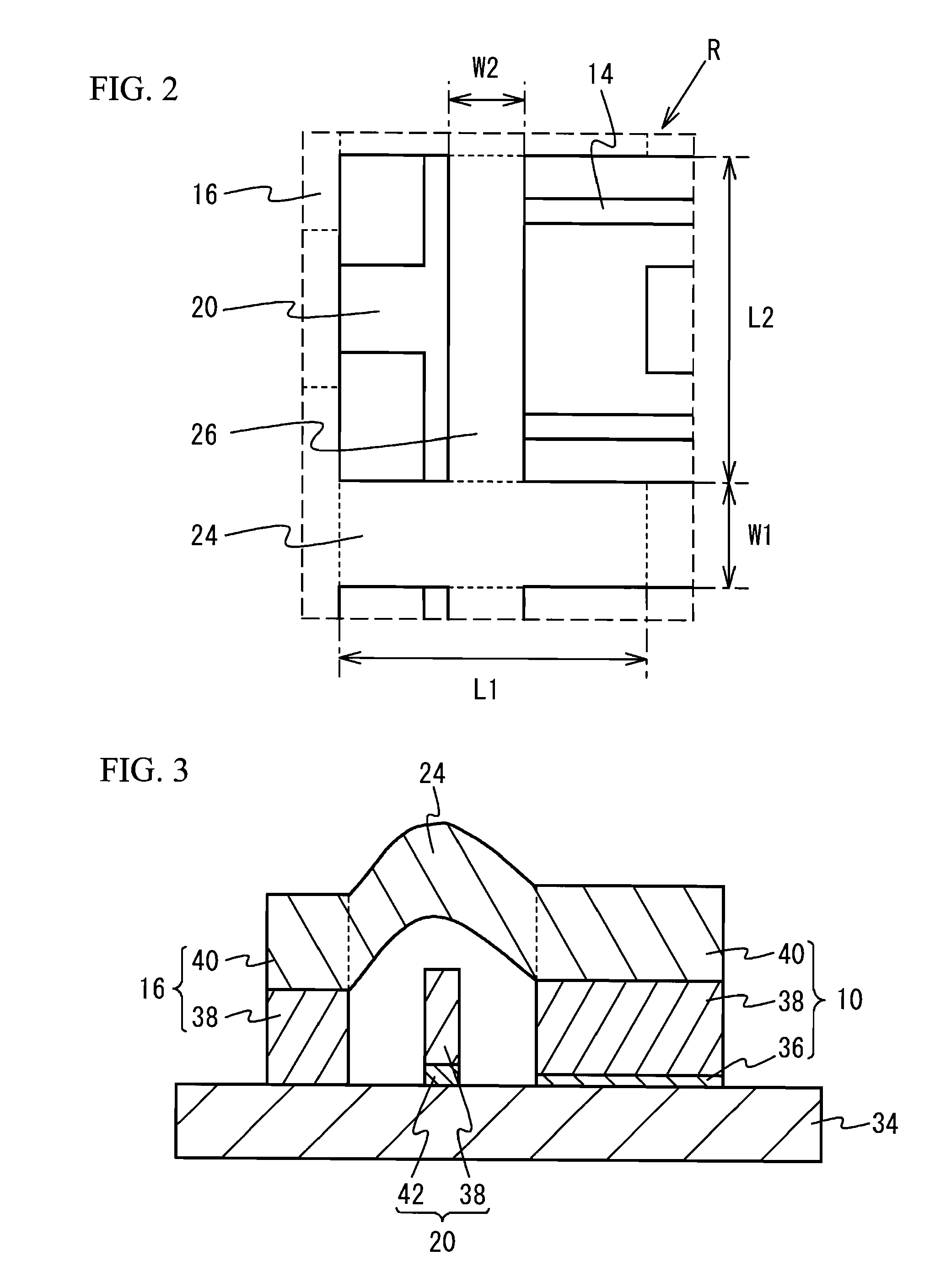
[0016]FIG. 1 is a schematic plan view of a semiconductor device in accordance with a first embodiment. FIG. 2 is an enlarged view of an area R indicated by a broken line in FIG. 1. The number of fingers is not limited to that illustrated in FIG. 1, but the semiconductor device has an arbitrary number of fingers. As illustrated in FIG. 1, the semiconductor device of the first embodiment has a plurality of source fingers 10, a plurality of drain fingers 12, and a plurality of gate fingers 14, which are provided on a semiconductor layer including a GaAs channel layer and an AlGaAs electron supply layer. The source fingers 10 are connected to a source bus line 16 that extends in a first direction (the vertical direction in FIG. 1), and are arranged in parallel with each other so as to extend from the source bus line 16 in a second direction that crosses the first direction at the right angle (the second direction is the horizontal direction in FIG. 1).

[0017]The drain fingers 12 are arra...

second embodiment

[0044]FIG. 6 is a schematic plan view of a semiconductor device in accordance with a second embodiment. The number of fingers is not limited to that illustrated in FIG. 6, but the semiconductor device has an arbitrary number of fingers. As illustrated in FIG. 6, the semiconductor device of the second embodiment third air bridges 48 that are located further out than the outermost source fingers 10a among the source fingers 10 in the first direction. Each of the third air bridges 48 is supported by the first air bridge 24 provided in the corresponding outermost source finger 10a at one end and by a fixing portion 50 provided in the semiconductor layer 34 at the other end. That is, the third air bridges 48 connect the fixing portions 50 and the outermost first air bridges 24. One end of each of the third air bridges 48 is supported by the center portion of the first air bridge 24 in the direction in which the first air bridge 24 extends. That is, the third air bridges 48 are connected ...


PUM


Abstract

A semiconductor device includes a semiconductor layer, an active region defined in the semiconductor layer, first fingers provided on the active region and arranged in parallel with respect to a first direction, second fingers provided on the active region and interleaved with the first fingers, a bus line that is provided on an outside of the active region and interconnects the first fingers, first air bridges that are provided on the outside of the active region and are extended over the bus line, and that are connected to the second fingers, and second air bridges that are provided on the outside of the active region and are arranged in a second direction which crosses to the first direction, and that interconnect the first air bridges.

Description

CROSS-REFERENCE TO RELATED APPLICATION[0001]This application is based upon and claims the benefit of priority of the prior Japanese Patent Application No. 2011-095345 filed on Apr. 21, 2011, the entire contents of which are incorporated herein by reference.BACKGROUND [0002](i) Technical Field[0003]A certain aspect of the embodiments discussed herein relates to semiconductor devices. Another aspect of the embodiments discussed herein relates to a semiconductor device having a multi-finger structure.[0004](ii) Related Art[0005]As semiconductor devices suitable for amplification in RF bands such as microwaves, quasi-millimeter waves or millimeter waves, there is a known a field effect transistor (FET) such as a high electron mobility transistor (HEMI).[0006]For example, Japanese Patent application Publication No. 8-172104 (Document 1) discloses an FET having a multi-finger structure having a plurality of gate fingers extending in parallel with each other, in which a source finger and a...

Claims


Application Information

Patent Timeline
Patent Type & Authority Applications(United States)
IPC IPC(8): H01L23/52
CPCH01L23/4821H01L23/4824H01L2924/0002H01L2924/00H01L29/41758
Inventor SHIMURA, TADAYUKI
Owner SUMITOMO ELECTRIC DEVICE INNOVATIONS
Why Eureka
Try Eureka