Supercharge Your Innovation With Domain-Expert AI Agents!

Substrate for organic electroluminescense device and method of manufacturing organic electroluminscense device employing same

a technology of organic electroluminescence and substrate, which is applied in the manufacture of electrode systems, electric discharge tubes/lamps, and luminescent screens of discharge tubes, etc., can solve the problem of difficult manufacturing process of organic electroluminescence devices using vacuum vapor deposition methods, and achieve the effect of suppressing deviation

Inactive Publication Date: 2012-10-25
SUMITOMO CHEM CO LTD
View PDF5 Cites 12 Cited by
  • Summary
  • Abstract
  • Description
  • Claims
  • Application Information

AI Technical Summary

Benefits of technology

The present invention provides a substrate for organic EL devices with a partition wall that partitions a coating area of ink applied on the pixel electrodes in parallel with each other, and a frame partition wall surrounding all of the pixel electrodes. The partition walls are designed to allow ink to flow between the communicated coating areas, resulting in a more even thickness of the organic EL layer and reduced luminance difference between pixels. The invention also provides a method for manufacturing the organic EL device with the substrate. The technical effect of the invention is to improve the quality of display apparatus and reduce the luminance difference between pixels.

Problems solved by technology

In this case, however, because of a problem with patterning precision of layers due to warping of the mask and a problem of high film-forming costs caused by the necessity of a large vacuuming apparatus, it has been considered that a manufacturing process for an organic EL device with a large screen by the use of the vacuum vapor deposition method is very difficult.

Method used


Image

  • Substrate for organic electroluminescense device and method of manufacturing organic electroluminscense device employing same
  • Substrate for organic electroluminescense device and method of manufacturing organic electroluminscense device employing same
  • Substrate for organic electroluminescense device and method of manufacturing organic electroluminscense device employing same

Examples


embodiment 1

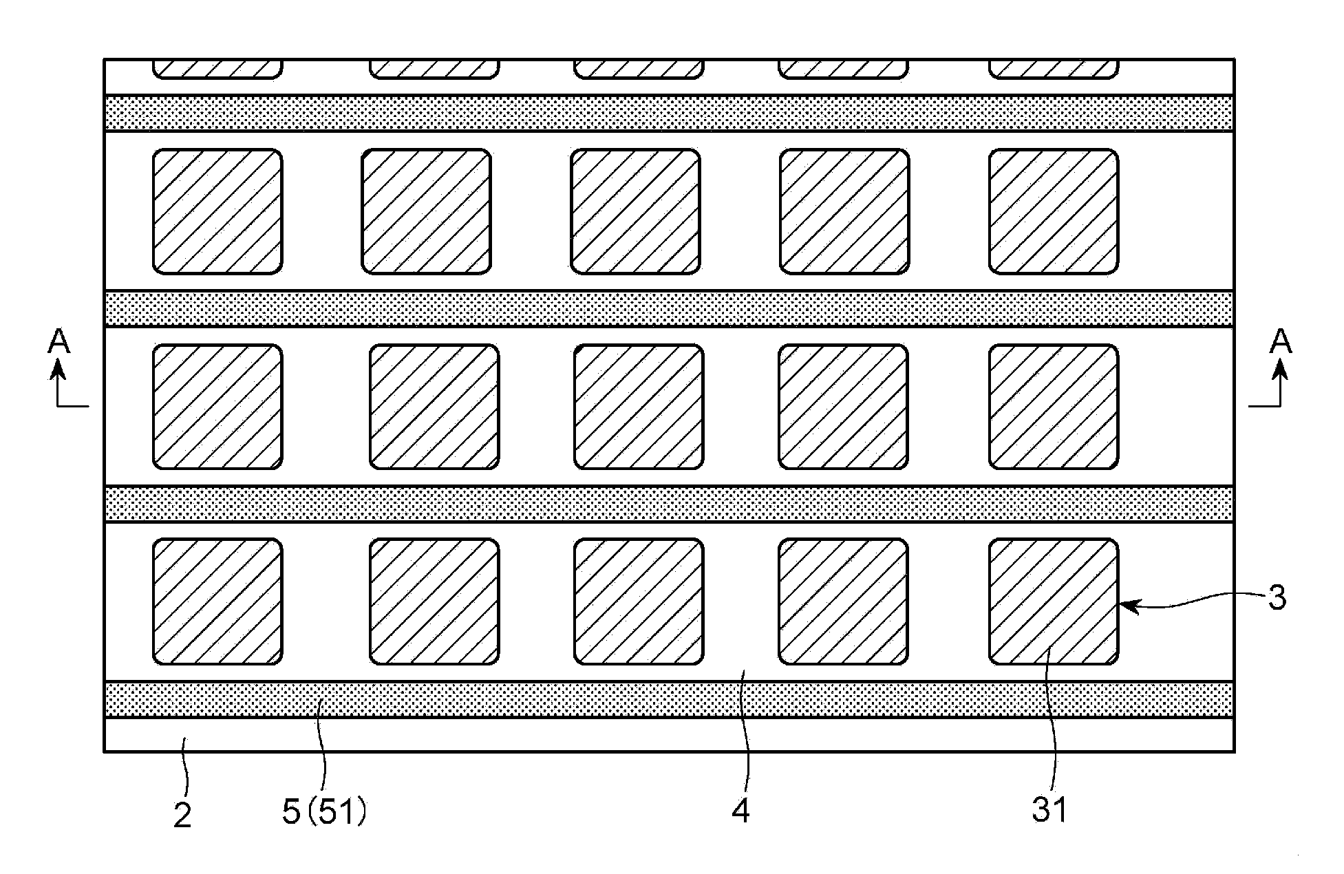
[0048]Referring to Figs., the following description will discuss a substrate for an organic EL device in accordance with embodiments of the present invention. In the Figures, a scale of each of members is sometimes different from an actual scale.

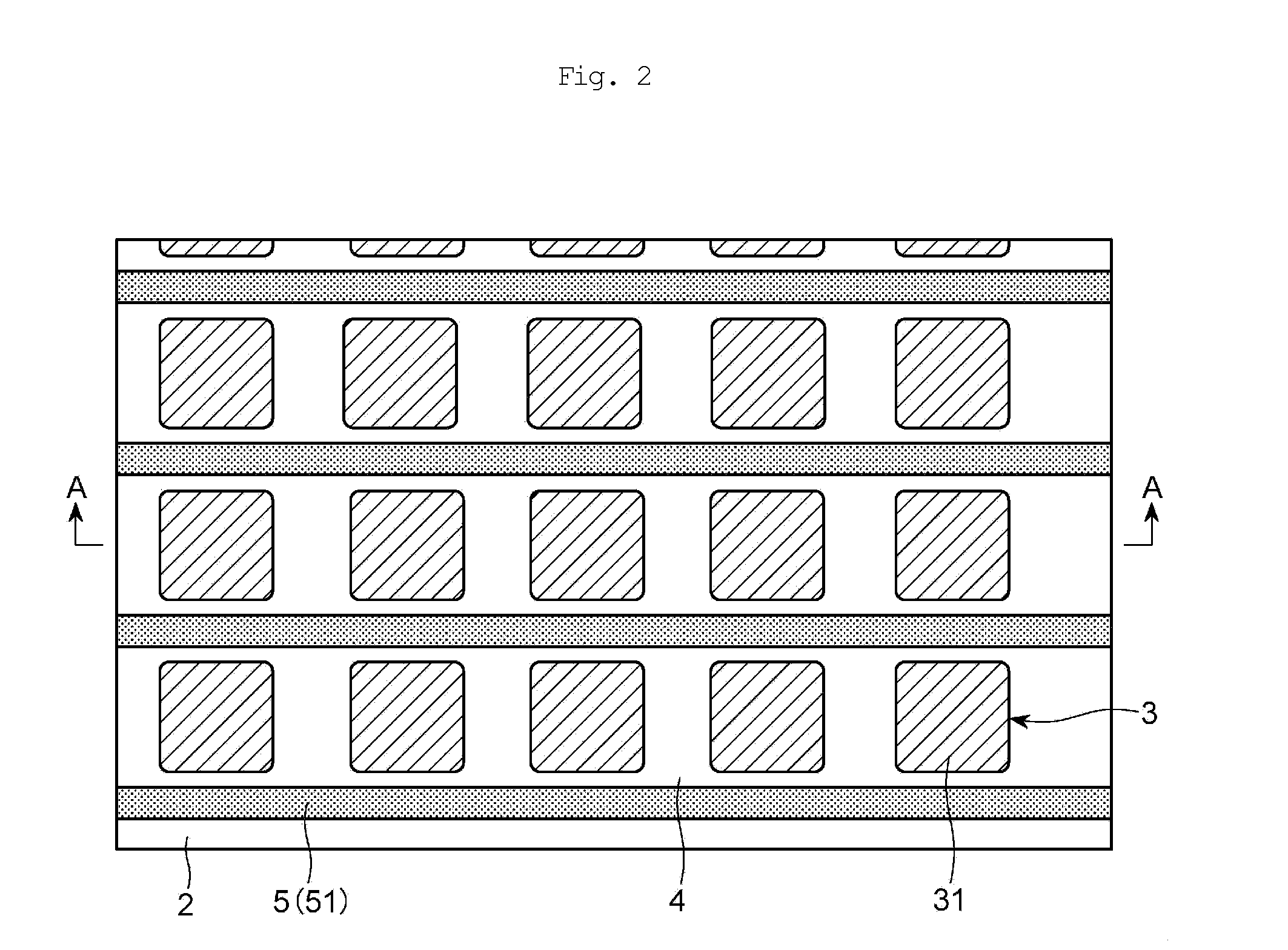
[0049]As shown in FIGS. 1 to 3, a substrate 1 for an organic EL device in the embodiment of the present invention is a substrate for use in mono-color light emission. The substrate 1 for an organic EL device is provided with a support substrate 2, a plurality of pixel electrode arrays 3 formed on the support substrate 2 in parallel with one another, pixel defining layers 4 for defining pixel electrodes 31 composed of the pixel electrode arrays 3, and partition walls 5 for defining an ink coating area S1 into a stripe pattern so as to form an organic EL layer containing a light emitting layer. Pixels refer to light emission areas defined by the pixel defining layers 4.

[0050]As the component material for the support substrate 2, any known mate...

embodiment 2

[0116]Referring to FIG. 8, the following description will discuss a substrate 1b for an organic EL device in accordance with embodiment 2 of the present invention. In FIG. 8, those members that are the same as those of FIG. 1 are indicated by the same reference numerals, and the description thereof will be omitted.

[0117]The substrate 1b for an organic EL device shown in FIG. 8 is used in the case when a light emission color of the light emitting layer is a mono color, and its notch 51a is formed only on one of the ends of each stripe partition wall 51. Neighboring coating areas S1 are communicated with each other only through one end portion side.

[0118]In the substrate 1b for an organic EL device, the coating areas S1, each formed into a stripe pattern, are communicated with each other by the notch 51a formed on one end of each stripe partition wall 51 so that the ink for use in forming an organic EL layer is allowed to flow between the communicated coating areas S1 from the area wi...

embodiment 3

[0119]Referring to FIG. 9, the following description will discuss a substrate 1c for an organic EL device in accordance with embodiment 3 of the present invention. In FIG. 9, those members that are the same as those of FIG. 1 are indicated by the same reference numerals, and the description thereof will be omitted.

[0120]In the substrate 1c for an organic FT, device shown in FIG. 9, between one end portion and the other end portion of each stripe partition wall 51, each of the notches 51a is alternately formed thereon.

[0121]Since the notches 51a are formed on the strip partition walls 51 in this manner, communications between the coating areas S1 can be made in accordance with the coating order of the nozzle 20 (see FIG. 5) that carries out a coating process on the coating areas S1 in a winding manner.


PUM


Abstract

The present invention provides a substrate for an organic EL device. The substrate for an organic EL device of the present invention is provided with a support substrate on which a plurality of pixel electrode arrays are formed in parallel with each other, and a partition wall composed of stripe partition walls located between each of the pixel electrode arrays along the pixel electrode arrays and a frame partition wall in the form of a rectangle surrounding all of the plurality of pixel electrode arrays, and in this structure, the partition wall partitions a coating area of ink applied on the pixel electrode arrays and a neighboring coating area of ink applied on the pixel electrode array, and notches are located in the stripe partition walls to make the neighboring coating areas communicate with each other.

Description

TECHNICAL FIELD[0001]The invention relates to a substrate for an organic electroluminescence (hereinafter, referred to as “organic EL”) device in which a partition wall that partitions pixels is formed on a support substrate, which is used for manufacturing organic EL devices, and also relates to a method for manufacturing an organic EL device using such a substrate.BACKGROUND ART[0002]Organic EL devices have already been put into practical use as devices for use in portable telephones and the like. The organic EL device includes an organic EL element made of a laminated article having an anode and a cathode and one or more organic EL layers including a light emitting layer sandwiched between these electrodes. The light emitting layer is made from an organic compound that emits light when, upon application of a voltage thereto, a current flows therethrough. The organic EL element has various characteristics. The organic EL element is formed by stacking thin films. By using the organ...

Claims


Application Information

Patent Timeline
Patent Type & Authority Applications(United States)
IPC IPC(8): H05K1/02H05B33/00H05B33/10
CPCH01L51/0005H01L27/3283H10K59/173H10K71/135Y10S428/917
Inventor FURIHATA, MASATOSHIAMAMIYA, SATOSHI
Owner SUMITOMO CHEM CO LTD
Features
  • R&D
  • Intellectual Property
  • Life Sciences
  • Materials
  • Tech Scout
  • Unparalleled Data Quality
  • Higher Quality Content
  • 60% Fewer Hallucinations
Learn More