Optical laminate, illuminating device, liquid crystal display device, and method for manufacturing optical laminate

a technology of optical laminate and illuminating device, which is applied in the direction of instruments, polarising elements, lighting and heating apparatus, etc., can solve the problems of high optical loss, increase in cost, and difficulty in reducing the thickness of backlight, and achieve the effect of less film thickness

Inactive Publication Date: 2012-10-25
SHARP KK
View PDF2 Cites 30 Cited by
  • Summary
  • Abstract
  • Description
  • Claims
  • Application Information

AI Technical Summary

Benefits of technology

[0028]In order to attain the above object, an optical laminate of the present invention is an optical laminate having a first indented pattern on its front surface and a second indented pattern on its back surface, said optical laminate, including: a first optical member including the first indented pattern; a second optical member including the second indented pattern; and a middle layer provided between the first optical member and the second optical member, the second optical member being less in film thickness than the first optical member, and the second optical member having a glass transition point lower than a glass transition point of the first optical member.
[0043]In order to attain the above object, a production method for an optical laminate of the present invention is a method of producing an optical laminate having a first indented pattern on its front surface and a second indented pattern on its back surface, the optical laminate comprising a first optical member including the first indented pattern, a se

Problems solved by technology

Therefore, it is difficult to reduce the thickness of the backlight 500.
This has been a cause of an increase in cost.
Further, there has been a problem in which, since the optical

Method used


Image

  • Optical laminate, illuminating device, liquid crystal display device, and method for manufacturing optical laminate
  • Optical laminate, illuminating device, liquid crystal display device, and method for manufacturing optical laminate
  • Optical laminate, illuminating device, liquid crystal display device, and method for manufacturing optical laminate

Examples


Embodiment Construction

[0055]The following description discusses embodiments of the present invention in detail.

[0056](Outline of Liquid Crystal Display Device)

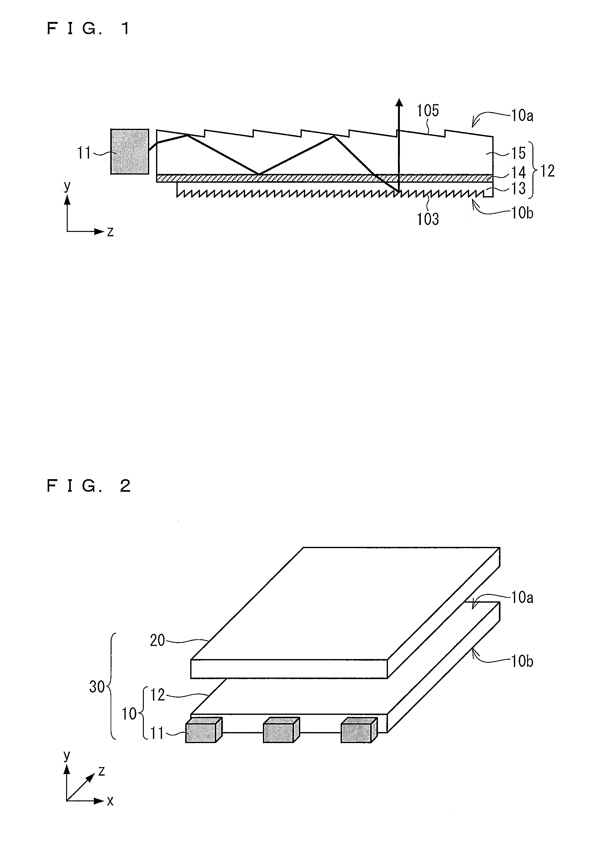
[0057]FIG. 2 is a perspective view illustrating a configuration of a liquid crystal display device 30 in accordance with the present embodiment.

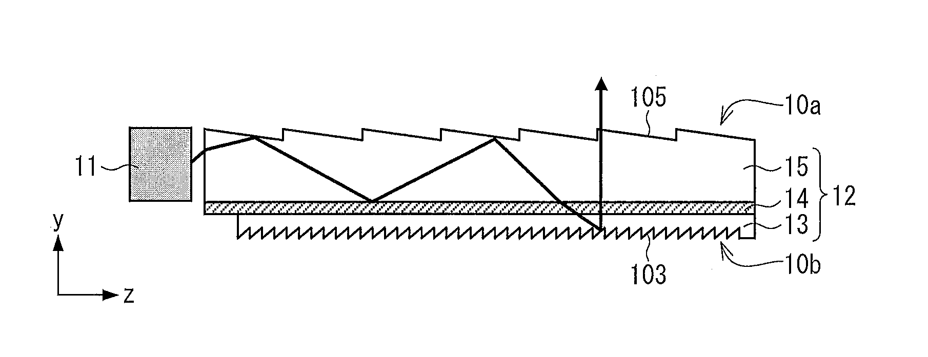
[0058]As illustrated in FIG. 2, the liquid crystal display device 30 includes a liquid crystal display panel 20 and a backlight 10 (illuminating device). The liquid crystal display panel 20 has a display screen for displaying an image. The backlight 10 emits light in the form of a plane to the liquid crystal display panel 20. A plurality of pixels for displaying an image are arranged in the liquid crystal display panel 20. The liquid crystal display panel 20 used here can be a known liquid crystal display panel.

[0059]The backlight 10 includes a plurality of light sources 11 and a light guide 12 (optical laminate) that is arranged so as to face the liquid crystal display panel 20. The backlight 10 is a side ...


PUM

PropertyMeasurementUnit
Temperatureaaaaaaaaaa
Glass transition temperatureaaaaaaaaaa

Abstract

An light guide (12) has an indented pattern (105) on its front surface (10a) and an indented pattern (103) on its back surface (10b), and includes: a light guide plate (15) including the indented pattern (105) provided on the front surface (10a); a light distribution control part (13) including the indented pattern (103) provided on the back surface (10b); and a middle layer (14) provided between the light guide plate (15) and the light distribution control part (13), the light distribution control part (13) being less in film thickness than the light guide plate (15), and the light distribution control part (13) having a glass transition point lower than that of the light guide plate (15). This makes it possible to form indented patterns on the front surface and the back surface of an optical laminate constituted by a stack of a plurality of layers, while preventing occurrence of defects.

Description

TECHNICAL FIELD[0001]The present invention relates to an optical laminate which emits light in the form of a plane, an illuminating device, and a method for manufacturing an optical laminate.BACKGROUND ART[0002]Conventionally, a side edge type backlight has been used as a backlight for use in a liquid crystal display device. Such a side edge type backlight is described with reference to FIG. 7.[0003]FIG. 7 is a view illustrating a configuration of a conventional side edge type backlight.[0004]As illustrated in FIG. 7, a backlight 500 is constituted by a stack of a reflecting plate 502, a light guide plate 503 and an optical film 504, which are arranged in this order from a back surface to a front surface. A light source 501 is provided on a side surface side of the light guide plate 503.[0005]The backlight 500 is configured such that, in order to allow light emitted from the light source 501 to enter the light guide plate 503 through the side surface and then travel inside the light...

Claims


Application Information

Patent Timeline
IPC IPC(8): G02F1/1335B32B37/14B32B38/06F21V7/00G02B5/30B32B7/023B32B7/027
CPCB29D11/00663Y10T156/1041B32B7/02B32B27/08B32B2307/412B32B2307/418B32B2457/202B32B2551/00G02B5/0215G02B6/0038G02B6/005G02B6/0053G02B6/0065G02F1/133615B32B3/30B32B7/023B32B7/027
Inventor KAIDA, KAZUYA
Owner SHARP KK
Why Eureka
Try Eureka