Topological Insulator-Based Field-Effect Transistor

a technology of topological insulators and field-effect transistors, applied in the direction of basic electric elements, electrical apparatus, semiconductor devices, etc., can solve the problems of inability to further scale supply voltages beyond, major roadblock to the improvement of computational capabilities and energy efficiency

Inactive Publication Date: 2012-11-01
BOARD OF RGT THE UNIV OF TEXAS SYST
View PDF3 Cites 48 Cited by
  • Summary
  • Abstract
  • Description
  • Claims
  • Application Information

AI Technical Summary

Benefits of technology

[0007]In accordance with a preferred embodiment of the present invention, a Topological INsulator-based field-effect transistor (TINFET) includes a first and second gate dielectric layers separated by a topological insulator (TI) layer. A first gate contact is connected to the first gate dielectric layer on the s

Problems solved by technology

Therefore, the inability to further scale supply voltages beyond this point represents a major roadblock to the conti

Method used


Image

  • Topological Insulator-Based Field-Effect Transistor
  • Topological Insulator-Based Field-Effect Transistor
  • Topological Insulator-Based Field-Effect Transistor

Examples


Embodiment Construction

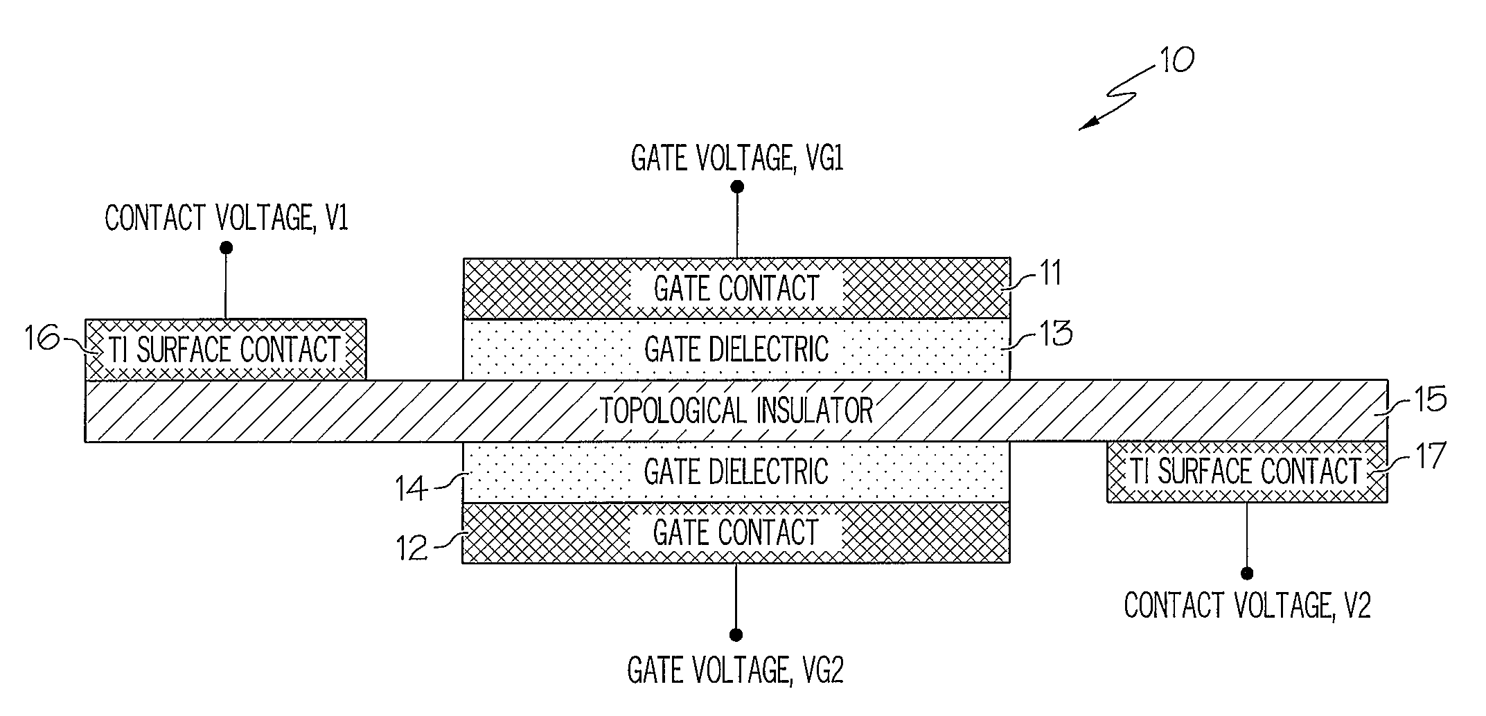
[0014]The present invention is related to a new type of transistor intended to allow improved performance at complementary metal-oxide semiconductor (CMOS) logic voltages and / or to allow lower voltage and power during operation than possible with CMOS logic. The new type of transistor, which can be called Topolgical INsulator-based FETs (TINFETs), is based on the concept of topological insulator (TI). TI is a new class of material that have a bulk insulating energy bandgap and robust, conducting quasi-two-dimensional surface states that lie within the energy range of the bulk energy bandgap. The conduction and valence bands of the TI surface state meet at a point in the Brillouin Zone commonly called the Dirac point.

[0015]In a perfect isolated TI layer, the Fermi level lies at the Dirac point such that these materials are semi-metallic. However, impurities, defects and surface contact effects with other materials may change the location of the Fermi level. These quantum Hall-like su...


PUM


Abstract

A Topological INsulator-based field-effect transistor (TINFET) is disclosed. The TINFET includes a first and second gate dielectric layers separated by a topological insulator (TI) layer. A first gate contact is connected to the first gate dielectric layer on the surface that is opposite the TI layer. A second gate contact may be connected to the second gate dielectric layer on the surface that is opposite the TI layer. A first TI surface contact is connected to one surface of the TI layer, and a second TI surface contact is connected to the second surface of the TI layer.

Description

STATEMENT OF GOVERNMENT INTEREST[0001]The present invention was made with United States Government support under NIST Award number 70NANB7H6168, awarded by the NIST. The United States Government has certain rights in the present invention.BACKGROUND OF THE INVENTION[0002]1. Technical Field[0003]The present invention relates to field-effect transistors in general, and in particular to topological insulator-based field-effect transistors.[0004]2. Description of Related Art[0005]For a metal-oxide-semiconductor field-effect transistor (MOSFET), the gate controls an electrical current flow between the source and drain by controlling the height of the conduction channel in energy below a threshold or through self-consistent electrostatics (i.e., the number of charge carriers within the channel above the threshold). Threshold is a point of switching between an ON state and an OFF state for a transistor. Above threshold in modem short channel devices (i.e., channel lengths of a few tens of ...

Claims


Application Information

Patent Timeline
IPC IPC(8): H01L29/66
CPCH01L49/003H10N99/03
Inventor BANERJEE, SANJAY K.REGISTER, II, LEONARD FRANKLINMACDONALD, ALLANSAHU, BHAGAWAN R.JADAUN, PRIYAMVADACHANG, JIWON
Owner BOARD OF RGT THE UNIV OF TEXAS SYST
Why Eureka
Try Eureka