Package structure having embedded electronic component and fabrication method thereof

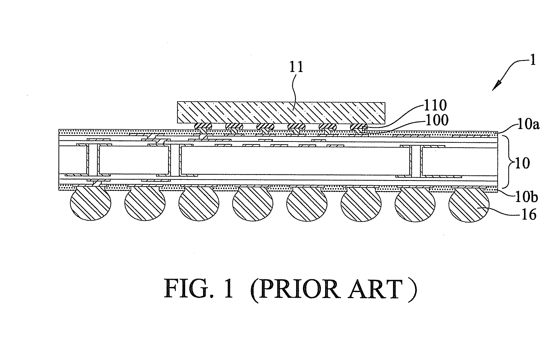
a technology of electronic components and packaging structures, applied in the direction of electrical equipment, semiconductor devices, semiconductor/solid-state device details, etc., can solve the problems of signal loss, package structure b>1/b> cannot meet the miniaturization requirement, and the pitch of the tin balls b>110/b> of the chip b>11/b> cannot be reduced, so as to avoid signal loss

Active Publication Date: 2012-11-01
UNIMICRON TECH CORP
View PDF1 Cites 12 Cited by
  • Summary
  • Abstract
  • Description
  • Claims
  • Application Information

AI Technical Summary

Benefits of technology

[0015]According to the present invention, the semiconductor chip is received in the cavity of the carrier and the solder material or conductive vias can be used for electrically connecting the wiring layer and the semiconductor chip such that the signal transmission path between the semiconductor chip and the carrier is shortened and only passes through one medium, thereby avoiding signal losses.
[0016]Further, since the semiconductor chip is embedded in the carrier, the pitch of the conductive vias or the solder material can be matched to the pitch of the solder bumps so as to allow the pitch of the solder bumps as well as the pitch of the wiring layer to be reduced according to requirements, thereby meeting the miniaturization requirement.

Problems solved by technology

However, since the circuit of the packaging substrate 10 has a small size, the pitch of the tin balls 110 of the chip 11 cannot be reduced.
As such, the package structure 1 cannot meet the miniaturization requirement.
Further, the solder bumps 100 of the packaging substrate 10 and the tin balls 110 of the chip 11 result in a too long signal transmission path between the chip 11 and the packaging substrate 10 and cause the signal transmission path to pass through different media (the solder bumps 100 and the tin balls 110), thereby easily resulting in signal losses.

Method used


Image

  • Package structure having embedded electronic component and fabrication method thereof
  • Package structure having embedded electronic component and fabrication method thereof
  • Package structure having embedded electronic component and fabrication method thereof

Examples


Embodiment Construction

[0020]The following illustrative embodiments are provided to illustrate the disclosure of the present invention, these and other advantages and effects can be apparent to those in the art after reading this specification.

[0021]It should be noted that the drawings are only for illustrative purposes and not intended to limit the present invention. Meanwhile, terms such as ‘up’, ‘down’, ‘a’ etc. are only used as a matter of descriptive convenience and not intended to have any other significance or provide limitations for the present invention.

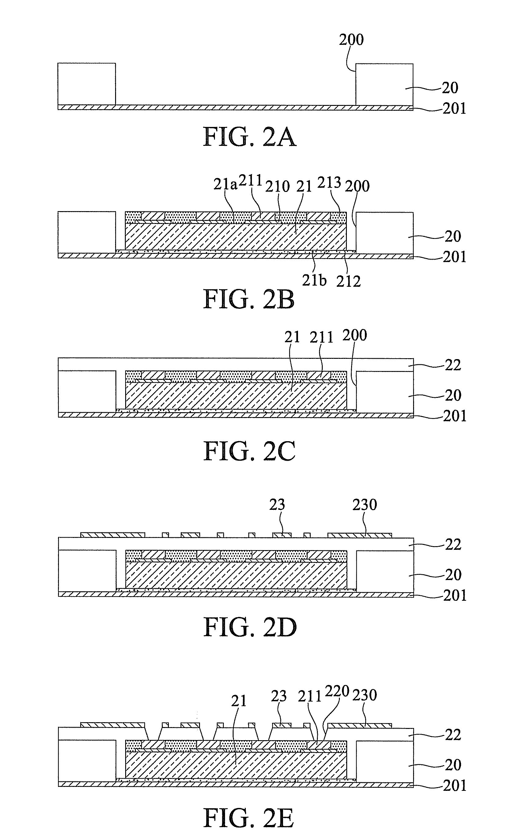
[0022]FIGS. 2A to 2G are cross-sectional views showing a fabrication method of a package structure having an embedded electronic component according to the present invention.

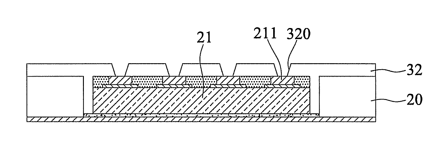
[0023]Referring to FIG. 2A, a carrier 20 having a cavity 200 penetrating therethrough is provided. The carrier 20 further has a metal layer 201 disposed at one side thereof for covering one end of the cavity 200. In the present embodiment, the carrier 20 is a copper-clad subst...


PUM


Abstract

A package structure having an embedded electronic component includes: a carrier having a cavity penetrating therethrough; a semiconductor chip received in the cavity and having solder bumps disposed thereon; a dielectric layer formed on the carrier and the semiconductor chip so as to encapsulate the solder bumps; a wiring layer formed on the dielectric layer; an insulating protection layer formed on the dielectric layer and the wiring layer; and a solder material formed in the dielectric layer and the insulating protection layer for electrically connecting the wiring layer and the solder bumps, thereby shortening the signal transmission path between the semiconductor chip and the carrier to avoid signal losses.

Description

BACKGROUND OF THE INVENTION[0001]1. Field of the Invention[0002]The present invention relates to package structures, and more particularly, to a package structure having an embedded electronic component and a fabrication method thereof.[0003]2. Description of Related Art[0004]Along with the progress of semiconductor packaging technologies, various package types have been developed for semiconductor devices so as to meet demands for highly integrated and minimized package structures. For example, wire-bonding packages or flip-chip packages allow semiconductor chips to be electrically connected to lead frames through gold wires or electrically connected to packaging substrates through solder bumps.[0005]FIG. 1 is a cross-sectional view of a conventional flip-chip package structure. The package structure 1 has a packaging substrate 10 having a chip-mounting surface 10a with solder bumps 100 disposed thereon and a ball-mounting surface 10b opposite to the chip-mounting surface 10a, a se...

Claims


Application Information

Patent Timeline
Patent Type & Authority Applications(United States)
IPC IPC(8): H01L23/48H01L21/56
CPCH01L23/13H01L24/14H01L23/5389H01L24/19H01L2224/131H01L2924/00013H01L23/49816H01L2224/12105H01L2924/01029H01L2224/13099H01L2224/13599H01L2224/05599H01L2224/05099H01L2224/29099H01L2224/29599H01L2924/014H01L2924/12042H01L2224/32245H01L2224/73267H01L2924/15153H01L2924/00
Inventor ZENG, ZHAO-CHONG
Owner UNIMICRON TECH CORP
Why Eureka
Try Eureka