

Printed circuit board and method of manufacturing the same
Patent Information
- Authority / Receiving Office
- US · United States
- Current Assignee / Owner
- NITTO DENKO CORP
- Publication Date
- 2012-11-08
Smart Images
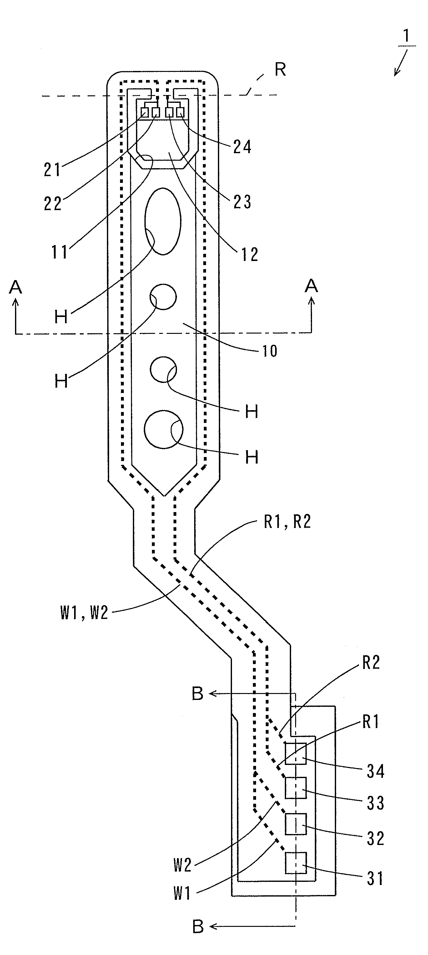
Figure 1 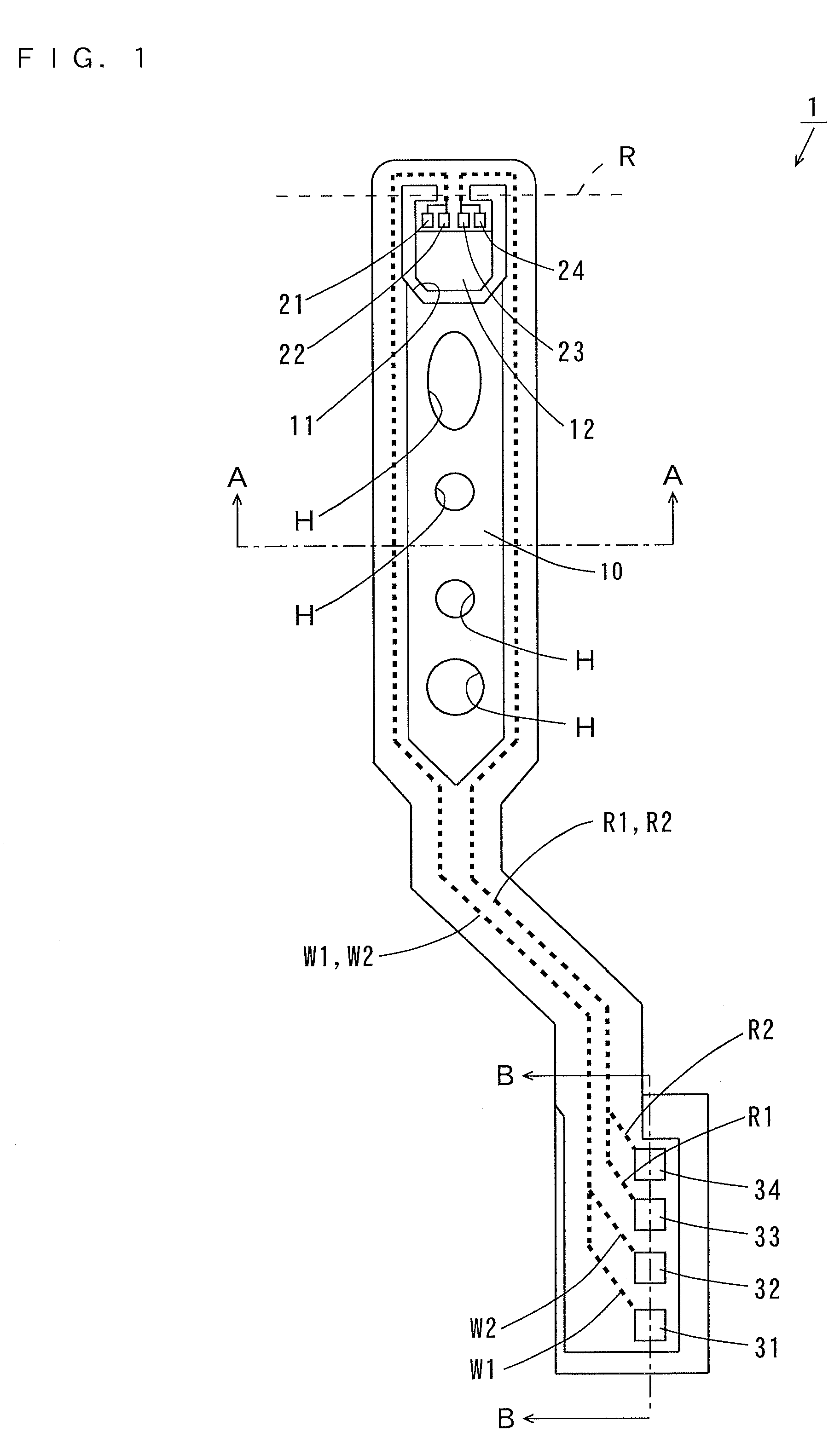
Figure 2 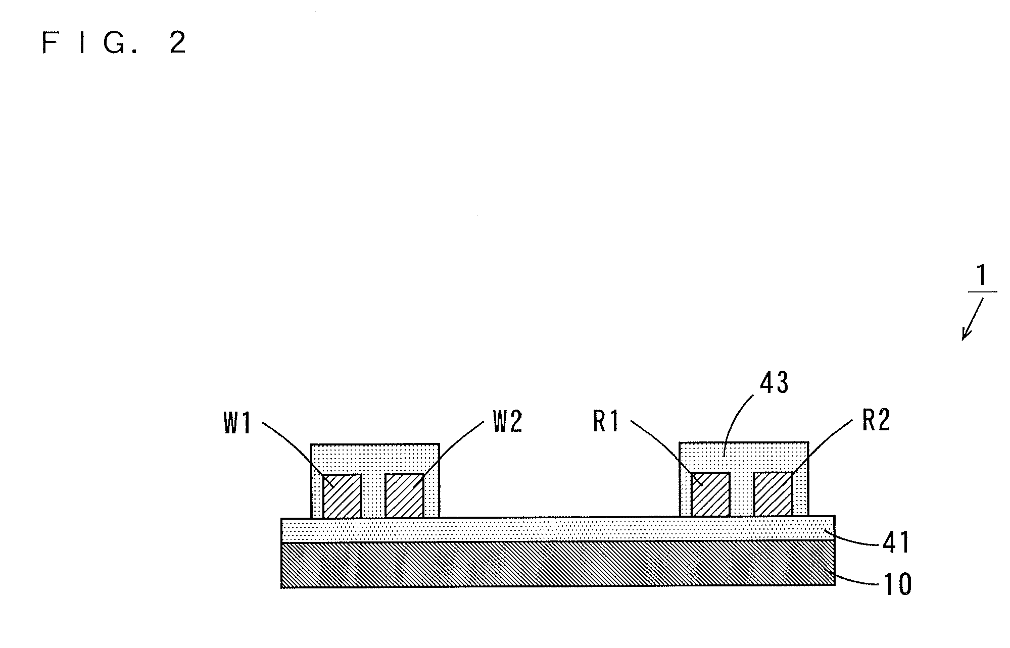
Figure 3
Abstract
Description
BACKGROUND OF THE INVENTION
[0001] (1) Field of the Invention
[0002] The present invention relates to a printed circuit board and a method for manufacturing the same.
[0003] (2) Description of Related Art
[0004] Actuators are used in drives such as hard disk drives. Such an actuator includes an arm provided rotatably around a rotation shaft, and a suspension board for a magnetic head that is attached to the arm. The suspension board is a printed circuit board for positioning the magnetic head at a desired track of a magnetic disk.
[0005] A suspension board with a circuit discussed in JP 2006-165268 A includes a conductor trace including a terminal for a magnetic head, a wiring, and a terminal for a relay. The terminal for a magnetic head in the suspension board with a circuit is connected to the magnetic head. The terminal for a relay in the suspension board with a circuit is connected to a relay flexible printed circuit board. Between the relay flexible printed circuit board and the magnetic...