Transparent photodetector

a photodetector and transparent technology, applied in the field of sensing devices, can solve the problems of change in electrical resistance of nanowires

Active Publication Date: 2012-11-08
GLOBALFOUNDRIES US INC
View PDF2 Cites 5 Cited by
  • Summary
  • Abstract
  • Description
  • Claims
  • Application Information

AI Technical Summary

Benefits of technology

[0003]The various advantages and, purposes of the exemplary embodiments as described above and hereafter are achieved by providing, according to a first aspect of the exemplary embodiments, a transparent photodetector. The transparent photodetector includes a substrate; a waveguide on the substrate; a displaceable structure that can move with respect to the substrate and is in proximity to the waveguide; and a silicon

Problems solved by technology

In operation, light propagating in the waveguide results in an optical force on the displaceable structure which further results in a strain on the nanowires to cause a change in electrical resistance of the nanowires.
In oper

Method used


Image

  • Transparent photodetector
  • Transparent photodetector
  • Transparent photodetector

Examples


Embodiment Construction

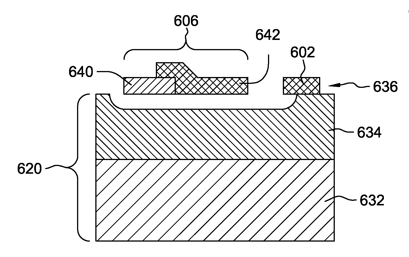
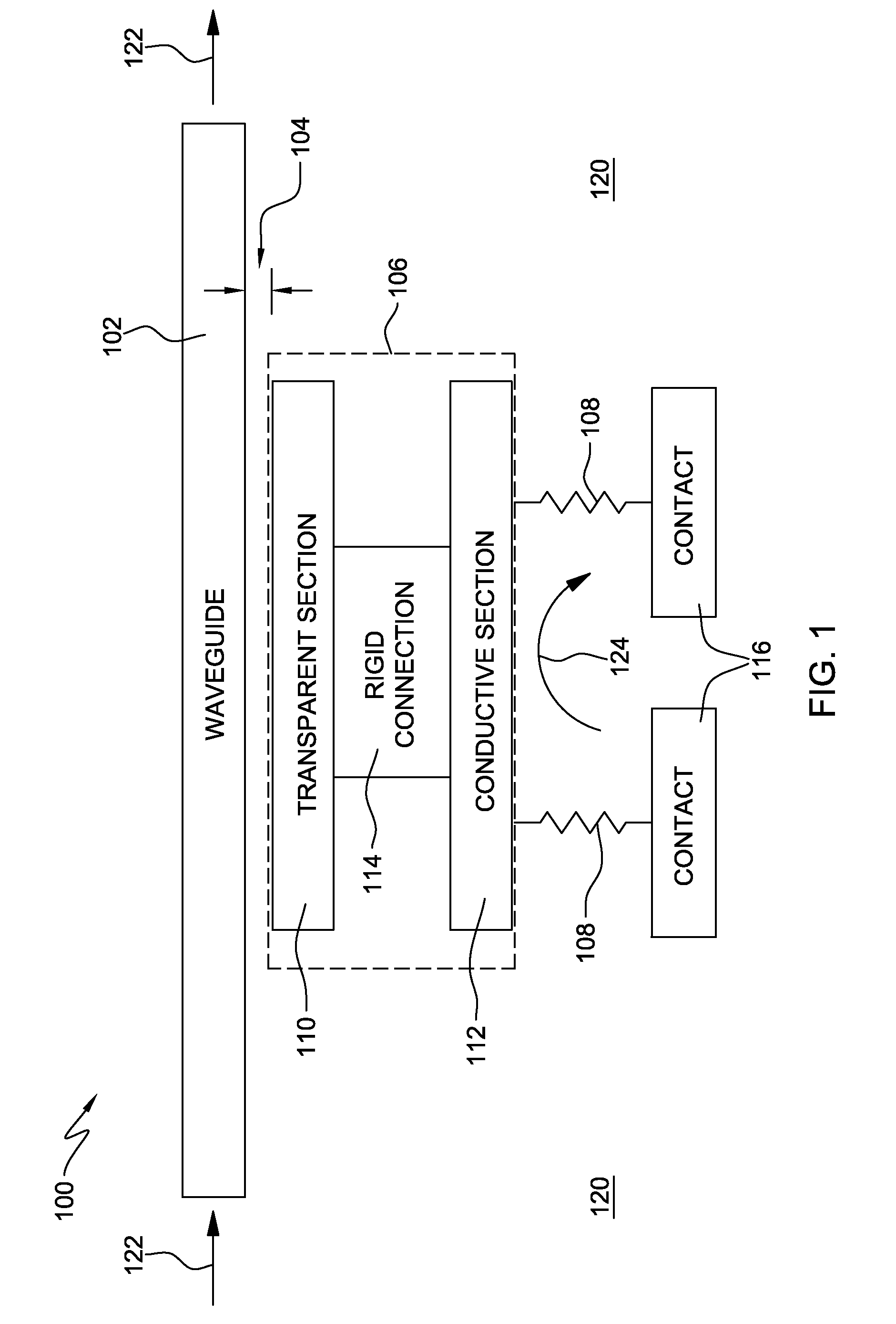
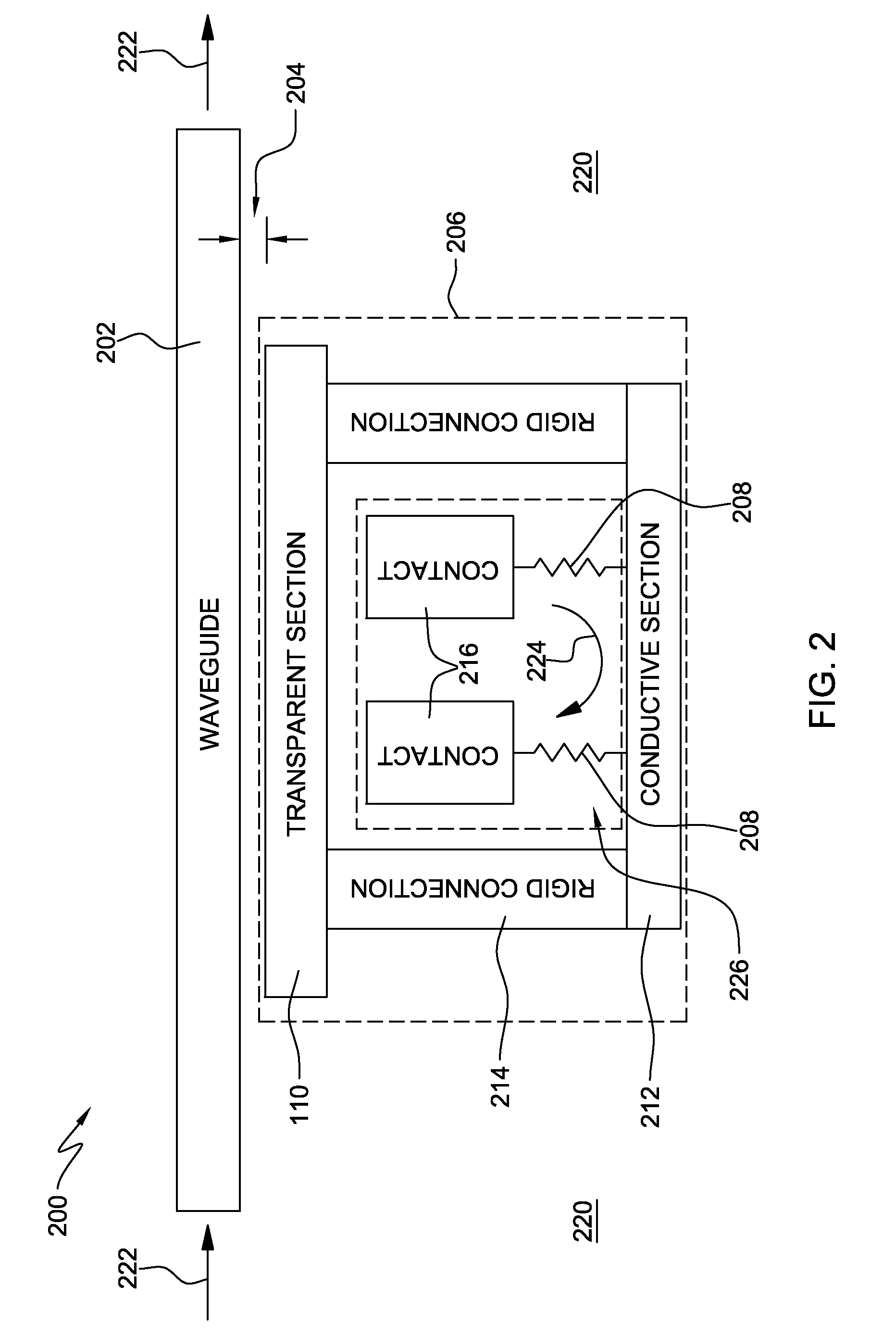
[0013]There is proposed a transparent photodetector in which there is a device capable of detecting light with negligible absorption of photons. The proposed device does not rely on carrier generation in semiconductors. Rather, the proposed device relies on optical forces and the large piezoresistance coefficient of silicon nanowires for detection of light.

[0014]The proposed transparent photodetector includes at least one waveguide, at least one displaceable structure in proximity to the waveguide and at least one silicon nanowire array mechanically linked to the displaceable structure. A silicon nanowire array means at least two nanowires.

[0015]Light propagating in the waveguide results in an optical force on the displaceable structure that is in proximity to the waveguide. The optical force may be attractive or repulsive. The applied optical force results in a strain on the nanowire array. The strain in the nanowire array changes the resistance of the nanowires through the enhance...


PUM


Abstract

A transparent photodetector. The transparent photodetector includes a substrate; a waveguide on the substrate; a displaceable structure that can be displaced with respect to the substrate, the displaceable structure in proximity to the waveguide; and a silicon nanowire array suspended with respect to the substrate and mechanically linked to the displaceable structure, the silicon nanowire array comprising a plurality of silicon nanowires having piezoresistance. In operation, a light source propagating through the waveguide results in an optical force on the displaceable structure which further results in a strain on the nanowires to cause,a change in electrical resistance of the nanowires. The substrate may be a semiconductor on insulator substrate.

Description

BACKGROUND[0001]The exemplary embodiments relate to sensing devices and, more particularly relate to photodetectors which can detect light with only negligible absorption of photons.[0002]Photodetectors are devices that translate light intensity into an electric signal. Photodetectors are widely used in optical communication systems from remote controls to fiber optic communication. Most photodetectors are semiconductor p-i-n junctions working on the principle of photon-induced carrier generation. Photons of energy larger than the semiconductor bandgap are absorbed by the semiconductor material. The absorption generates electron-hole pairs that are then detected by measuring the resulting current.BRIEF SUMMARY[0003]The various advantages and, purposes of the exemplary embodiments as described above and hereafter are achieved by providing, according to a first aspect of the exemplary embodiments, a transparent photodetector. The transparent photodetector includes a substrate; a waveg...

Claims


Application Information

Patent Timeline
IPC IPC(8): H01L31/0352B82Y20/00
CPCG01J1/42B82Y20/00H01L31/035227H01L31/08
Inventor BARWICZ, TYMON
Owner GLOBALFOUNDRIES US INC
Why Eureka
Try Eureka