Component

a technology of components and components, applied in the field of components, can solve problems such as space-saving electrical conta

Active Publication Date: 2012-11-08
ROBERT BOSCH GMBH
View PDF4 Cites 29 Cited by
  • Summary
  • Abstract
  • Description
  • Claims
  • Application Information

AI Technical Summary

Benefits of technology

[0008]In deviation from the side-by-side chip arrangement known from the related art, the packaging concept according to the present invention is based on a stacked arrangement of semiconductor component and MEMS component, whereby the lateral dimensions of the component may be clearly reduced. Furthermore, the packaging concept according to the present invention provides a flip-chip mounting of the MEMS component on the carrier. Using this connecting technology, the MEMS component is able to be mechanically fixed very simply at a standoff from the carrier surface, so that the diaphragm function of the MEMS component is assured. In addition, flip-chip mounting enables an extremely space-saving electrical contacting of the MEMS component. Based on the face-down orientation of the MEMS component, the carrier forms a mechanical protection for the front side of the component having the micromechanical diaphragm structure. The backside of the MEMS component having the cavity is at least partially covered by the additional semiconductor component, and is thus protected from negative environmental influences. All in all, the packaging concept according to the present invention offers very great flexibility, as far as the type, form and material of the housing are concerned, as well as the positioning of the front and back volumes.
[0010]Because of the connection to the MEMS component, the additional semiconductor component is in a stable insertion position, which is relatively far from the carrier. In addition, the semiconductor component and the carrier are relatively well mechanically decoupled, based on the flip-chip mounting of the MEMS component. Because of that, a thermomechanically conditioned bending of the semiconductor component is largely prevented. This is of advantage particularly in the case of ASIC's, since in this case mechanically conditioned strains in the component are able to lead to an undesired signal drift.
[0012]However, with the aid of the additional semiconductor component, a defined access or pressure connection to the backside of the diaphragm structure may be created, for instance, when the semiconductor component has a smaller chip area than the MEMS component and / or is situated offset to it, so that the semiconductor component spans the backside cavity of the MEMS component only partially. Alternatively, however, the semiconductor component may also be provided with at least one through hole, which is situated so that it opens out into the backside cavity of the MEMS component. For this, methods such as trenching are available, using which, the dimensions and also the positions of through holes are able to be specified very accurately. Thereby very small through holes are able to be implemented, having a diameter in the pm range.
[0014]In one specific embodiment of the present invention, beside the carrier, the housing includes a cover part positioned over the chip stack and is connected to the carrier in a circumferentially pressure-tight manner. Such a cover part may be adapted very simply in material, shape and size, to the application-specific requirements of the component. As an example, we mention here a component having a MEMS microphone component. The microphone performance is able to be substantially affected by the embodiment of the cover part, since the housing cover codetermines the size ratios of front and backside volumes. In this application, it proves advantageous if the sound opening in the cover part is connected pressure-tight to a through hole in the semiconductor component, so that the backside of the diaphragm structure is acted upon by the sonic pressure, and only the backside cavity of the MEMS component functions as a front volume, while the comparatively large housing cavity between the carrier and the cover part is connected to the front side of the diaphragm structure and is available as a backside volume.

Problems solved by technology

In addition, flip-chip mounting enables an extremely space-saving electrical contacting of the MEMS component.

Method used


Image

  • Component
  • Component
  • Component

Examples


Embodiment Construction

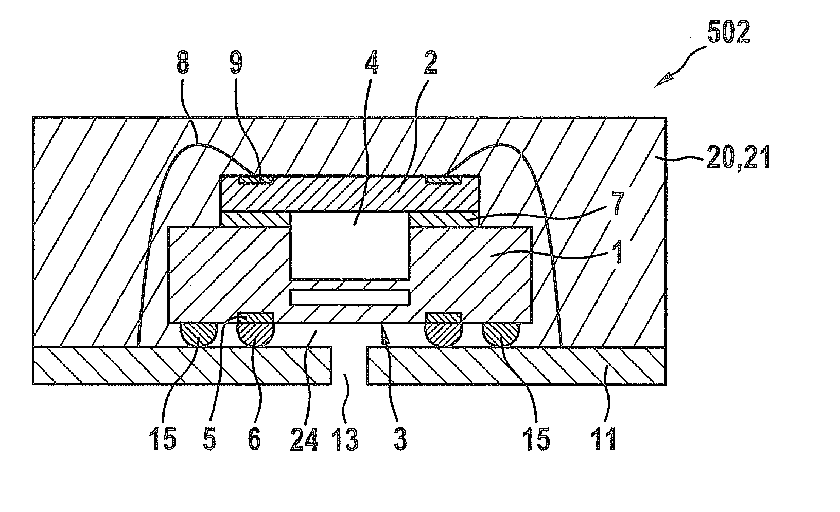
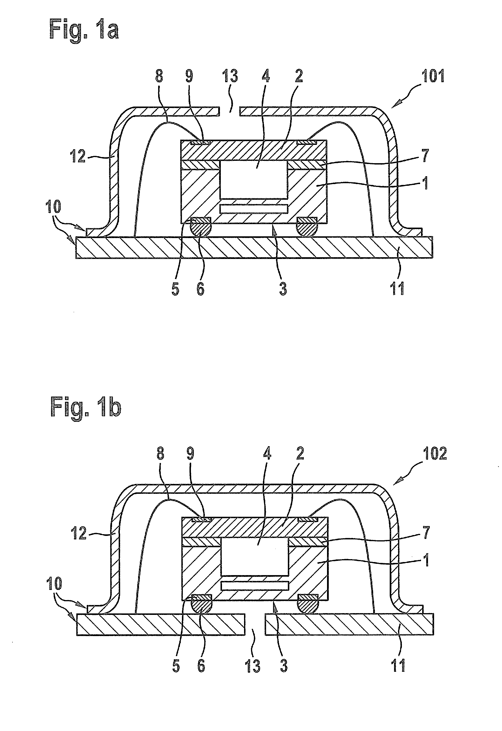
[0025]In the figures, the same reference numerals are used for the same components of the component design.

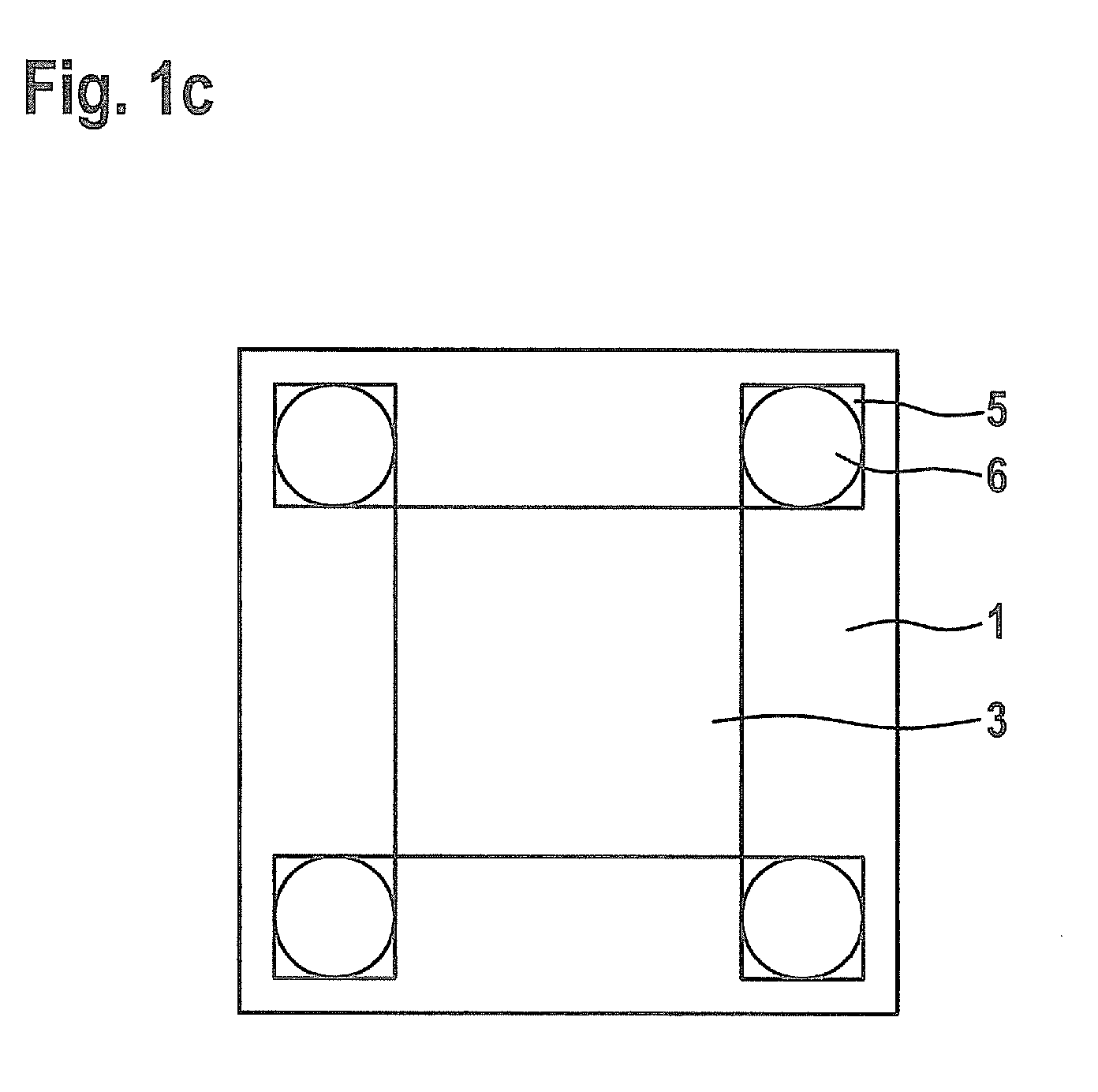
[0026]All the exemplary embodiments refer to a component having a MEMS microphone component 1 and an ASIC 2 as the additional semiconductor component. At the front side of microphone component 1 there is developed a diaphragm structure 3 having means for signal detection, which are contacted via four connection pads 5 on the front side of microphone component 1. Diaphragm structure 3 spans a cavity 4 in the component backside.

[0027]Microphone component 1 is mounted in flip-chip technique, that is, using its front side on a carrier 11, so that there is a gap between diaphragm structure 3 and the carrier surface (standoff). Carrier 11 may, for example, be a printed circuit board substrate in the form of a multi-panel substrate. The solder flip-chip technique is particularly suitable as mounting technique. However, adhesion flip-chip technique may also be used.

[0028]ASIC 2 is situ...


PUM


Abstract

A component includes at least one MEMS component and at least one additional semiconductor component in a common housing having at least one access opening. On the front side of the MEMS component, at least one diaphragm structure is provided, which spans a cavity on the backside of the MEMS component. The housing includes a carrier, on which the MEMS component is mounted. The MEMS component is mounted, using its front side, on the carrier, so that there is a standoff between the diaphragm structure and the carrier surface. The at least one additional semiconductor component is connected to the backside of the MEMS component, so that the MEMS component and the semiconductor component form a chip stack.

Description

BACKGROUND OF THE INVENTION[0001]1. Field of the Invention[0002]The present invention relates to a component having at least one MEMES component and at least one additional semiconductor component, which are situated in a common housing having at least one access opening; on the front side of the MEMES component, at least one diaphragm structure is developed which spans a cavity in the backside of the MEMS component; and the housing includes a carrier on which the MEMS component is mounted.[0003]2. Description of the Related Art[0004]In practice, such carriers or substrate-based housings are used for packaging MEMS microphone components. In this case, the microphone chip is mounted on a carrier, using chip-on-board (COB) technology, contacted electrically and housed using a cover. Usually, the microphone chip is mounted with its backside on the carrier, so that the cavity below the diaphragm structure is closed by the carrier. If the sound opening is located in the housing cover, th...

Claims


Application Information

Patent Timeline
Patent Type & Authority Applications(United States)
IPC IPC(8): H01L29/84
CPCH01L24/32H01L24/48H01L2924/07802H01L24/73H04R19/04H01L2224/32145H01L2224/48225H01L2224/73265H01L2924/1433H01L2924/1461H01L2924/15151H01L2924/16151H01L2224/32225H01L2924/18161H04R19/005B81B7/02B81B3/00H01L25/16B81B7/0061B81C1/0023B81B2201/0257B81B2207/015H01L2924/00H01L2224/48227H01L2224/16225H01L2224/16245H01L2224/48091H01L2224/48247H01L2924/10155H01L2924/181H01L2924/10157H01L2924/10158H01L2924/1815H01L2924/00014H01L2924/00012H01L2224/45099H01L2224/45015H01L2924/207
Inventor ZOELLIN, JOCHENEHRENPFORDT, RICARDOSCHOLZ, ULRIKE
Owner ROBERT BOSCH GMBH
Why Eureka
Try Eureka