Light Emitting Diode Light Source With Layered Phosphor Conversion Coating

Inactive Publication Date: 2012-11-15
SHENG FANG +1
View PDF2 Cites 62 Cited by
  • Summary
  • Abstract
  • Description
  • Claims
  • Application Information

AI Technical Summary

Benefits of technology

[0011]Implementations may include one or more of the following features. Additional phosphor layers may be deposited to form the phosphor conversion coating. For example, a third phosphor layer can be deposited over the second phosphor layer. The first and the third phosphor layers may be of the same materials and may be separated from each

Problems solved by technology

Though appearing an ideal solution for a white LED light source, Approach A has not been in practical use.
This is due to the following reasons: the complexity of the light source system, the high cost of such a complicated system, and the efficiency gaps between the three colored LEDs that makes the overall efficiency of the system lower.
Adding phosphors with red emission may improve the color rendering (higher color rendering index, or CRI), but it comes at the price of sacrifi

Method used


Image

  • Light Emitting Diode Light Source With Layered Phosphor Conversion Coating
  • Light Emitting Diode Light Source With Layered Phosphor Conversion Coating
  • Light Emitting Diode Light Source With Layered Phosphor Conversion Coating

Examples


Embodiment Construction

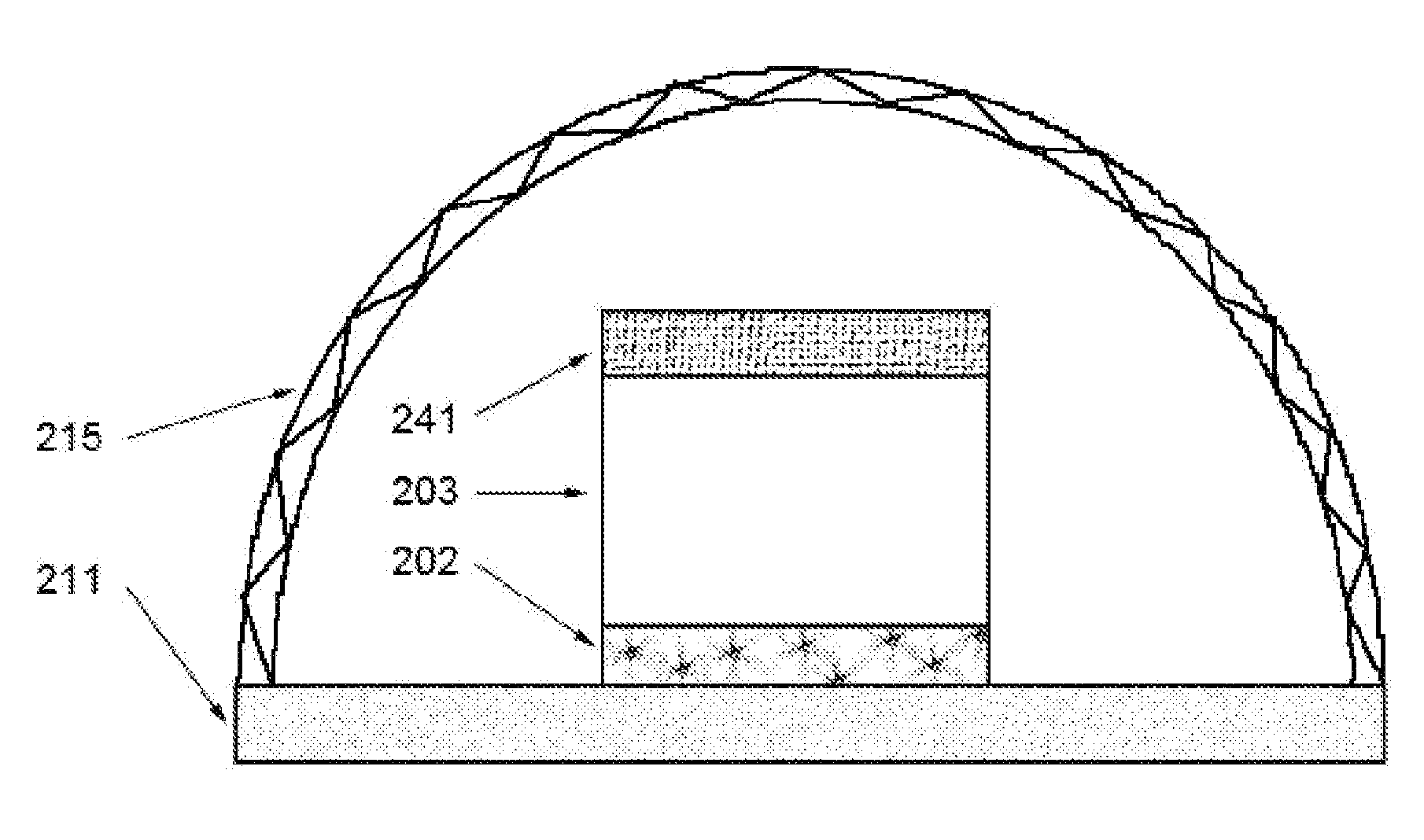
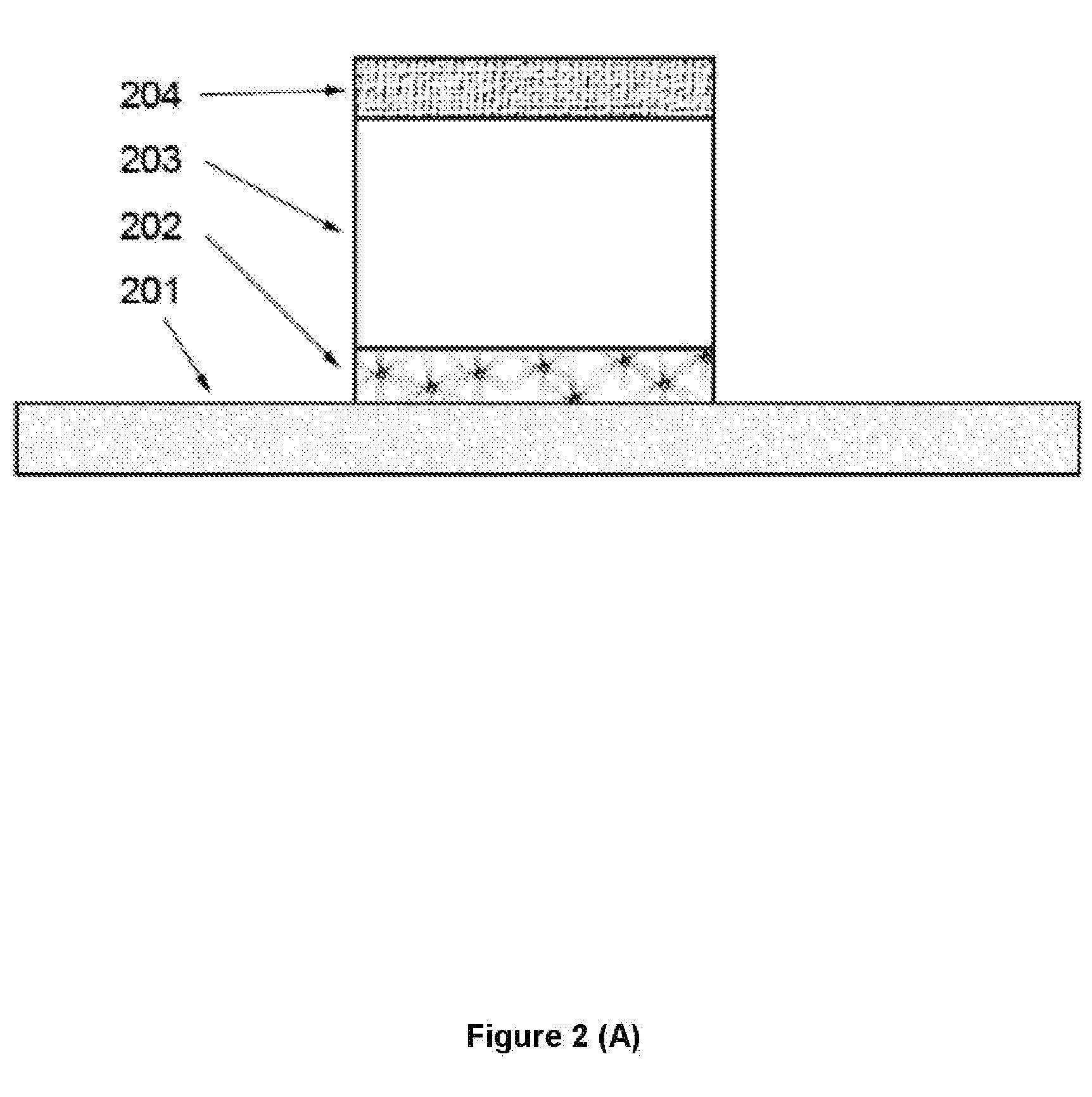
[0016]FIGS. 2A-2D show phosphor conversion LEDs that include a substrate 201 (or 211, or 221, or 231), a layer of solder 202 (or 212, or 222, or 232), an LED chip (junction) 203 (or 213, or 223, or 233), a phosphor conversion coating 204 (or 214, or 224, or 234), and / or an optical lens 215 (or 225, or 235). The LED junction 203 (or 213, or 223, or 233) can be a single LED chip (junction) or an array of LED chips. The layer of solder is used to connect LED chip(s) to the substrate 202 (or 212, or 222, or 232). The substrate should be an electrical insulator. The phosphor conversion coating 204 can be placed directly on the top of LED chip 201, as shown in FIG. 2A and FIG. 2B, or placed on the inner surface of the optical lens 225 (or 235), as shown in FIG. 2C and FIG. 2D. The optical lens 225 (or 235) is used for better light distribution emitted from the system.

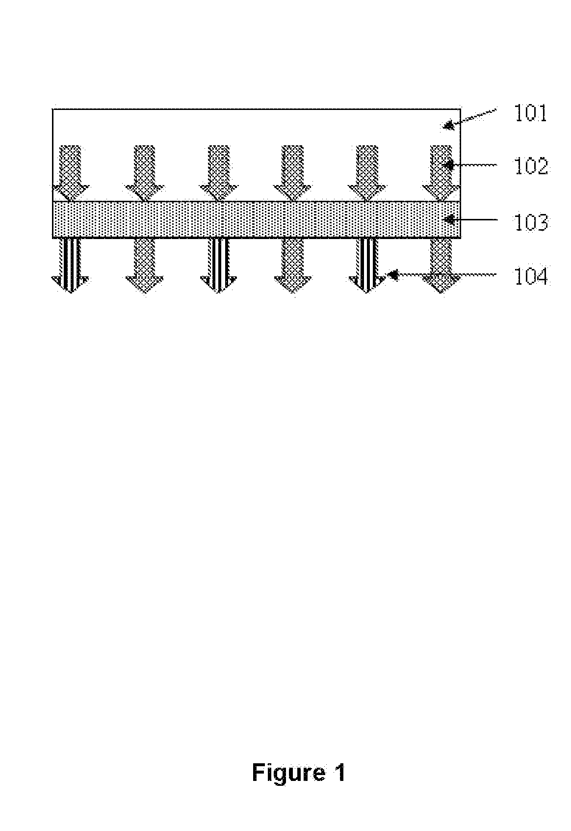
[0017]The phosphor conversion coating 204 (or 214, or 224, or 234) can be formed by depositing phosphor materials directly ...


PUM


Abstract

The LED (light emitting diode) light source that includes an LED chip or an array of LED chips that emit blue, or UV, violet, or other narrow wavelength light and a phosphor conversion coating that absorbs the radiation from the LED and re-emits lights of longer wavelengths and with wider spectrum of wavelength. The phosphor conversion coating includes a plurality of layered phosphor films wherein adjacent phosphor films are formed of different phosphor materials. A method of forming an LED light source includes soldering LED chip to an electrically insulating substrate and forming a phosphor conversion layer. Forming the phosphor conversion layer includes depositing a number of adjacent phosphor films directly on the surface of the LED chip or on the surface of an optically transparent substrate which may be of curved or flat surface.

Description

BACKGROUND[0001]Light emitting diode (LED) was invented almost ninety years ago and has been receiving a great deal of attention since. In particular, the discovery of blue light LED in 1990s has led to a drastic improvement in conversion efficiency of electric energy to light. This has made it possible to use LED for general lighting purpose. In fact, the recent years has witnessed rapid adoption of LED in many applications, including general lighting, automobile lighting, cell phone keyboard lighting, and flat TV edge lighting. The main reasons for such rapid adoption are that (1) an LED light can be much more efficient than traditional lighting sources such as incandescent light bulbs or fluorescent tubes, (2) it can have much longer service lifetime, (3) it is more flexible and can be made into any shape to fit any lighting space requirement, and (4) it is made of materials benign to the environment.[0002]Since the light generated from an LED is determined by the bandgap energy ...

Claims


Application Information

Patent Timeline
IPC IPC(8): H05B33/12
CPCC09K11/7731C09K11/7774H01L33/504C09K11/77347C09K11/77342C09K11/77348
Inventor YANG, LIUSHENG, FANG
Owner SHENG FANG
Why Eureka
Try Eureka