Transistor outline (TO)-CAN packaged semiconductor laser and fabrication method thereof

A TO-CAN and semiconductor technology, applied in the laser field, can solve the problems affecting the quality stability of laser products, increase the application of high-cost gold wire, and the complicated bonding operation process, so as to simplify the gold wire bonding operation process and save The cost of bonding gold wire and the effect of improving the quality of light output

Inactive Publication Date: 2016-01-20
武汉海赛姆光电技术有限公司
View PDF5 Cites 17 Cited by
  • Summary
  • Abstract
  • Description
  • Claims
  • Application Information

AI Technical Summary

Problems solved by technology

However, in this kind of TO-CAN packaged semiconductor laser, which is the mainstream of the industry, there are the following defects in the packaging operation of connecting the PD chip as the backlight detector to the corresponding pin through two gold wire bonding: the PD chip is used twice Gold wire bonding makes the bonding process relatively complicated, and increases the application of high-cost gold wires, which increases the overall cost of the laser to a certain extent and reduces the market competitive advantage; and for PD chips, special settings are required. The installation of the detection chip pad not only complicates the installation process, but also the detection chip pad and the TO tube seat are fixed with silver glue, which has the risk of falling off, which directly affects the quality stability of the laser product
Therefore, the TO-CAN package semiconductor laser in the prior art still has certain defects in the setting of the backlight detector chip and the packaging process operation, and there is still room for improvement.

Method used


Image

  • Transistor outline (TO)-CAN packaged semiconductor laser and fabrication method thereof
  • Transistor outline (TO)-CAN packaged semiconductor laser and fabrication method thereof
  • Transistor outline (TO)-CAN packaged semiconductor laser and fabrication method thereof

Examples


Embodiment Construction

[0038] The technical solution of the present invention will be described in detail below in conjunction with the accompanying drawings, so that those skilled in the art can clearly understand the present invention, but the protection scope of the present invention is not limited thereby.

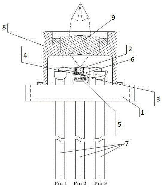
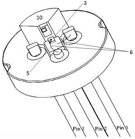
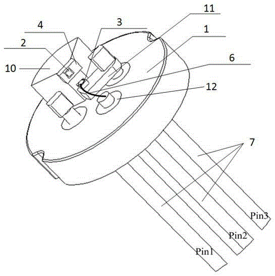
[0039] TO-CAN packaged semiconductor laser is currently widely used as a communication light source device, and its structure is constantly being optimized and developed. This invention is based on long-term innovative experimental research, and proposes a TO-CAN packaged semiconductor laser with a new structure, which greatly improves The comprehensive performance of TO-CAN packaged semiconductor laser is shown, as attached image 3 As shown, the TO-CAN packaged semiconductor laser of the present invention includes a TO socket 1, a semiconductor laser chip 2, a backlight detector chip 3, a laser chip spacer 4, a bonding gold wire 6, a pin 7, a heat sink block 10, Support table 11, TO tube c...


PUM


Abstract

The invention proposes a transistor outline (TO)-CAN packaged semiconductor laser and a fabrication method thereof. The TO-CAN packaged semiconductor laser comprises a TO tube base, a semiconductor laser chip, a backlight detector chip, a gold bonding wire, pins and a heat sink block, wherein the heat sink block is arranged on the upper surface of the TO tube base, the pins are fixed on the TO tube base in an insulation way, the upper end of at least one pin protrudes out of the upper surface of the TO tube base, the semiconductor laser chip is fixed on the surface of the heat sink block, the upper part of the pin protruding out of the upper surface of the TO tube base is connected with a support table, and the backlight detector chip is arranged on the support table and below the semiconductor laser chip. In the TO-CAN packaged semiconductor laser, the backlight detector chip is arranged on the support table integrated and connected with the pins, thus, an independent cushion block is omitted, and the material cost of the cushion block is saved; and moreover, the gold wire bonding process between the backlight detector chip and the cushion block in one time is omitted, the gold wire bonding process is simplified, the gold wire bonding cost is saved, and the stability of a laser product is improved.

Description

technical field [0001] The present invention relates to the field of laser technology, and more specifically relates to a TO-CAN packaged semiconductor laser and a manufacturing method thereof. Background technique [0002] TO packaging, Transistor Outline or Through-hole packaging technology, belongs to the packaging structure of coaxial optical transmission devices. It is developed from the original widely used transistor device packaging and is relatively mature in the industry. The parasitic parameters of the TO package are small, the process is simple, the cost is low, and it is flexible and convenient to use. Currently, the LD package with a rate below 10G mainly adopts the TO package. In the LD package, the internal space of the TO shell is small, and there are only four leads, and no semiconductor cooler (TEC) is installed, which also has a great advantage in cost. The material used for the TO tube shell is mainly stainless steel or valve. The entire structure of th...

Claims


Application Information

Patent Timeline
Patent Type & Authority Applications(China)
IPC IPC(8): H01S5/022
Inventor 李林森鲁杰肖黎明
Owner 武汉海赛姆光电技术有限公司
Why Eureka
Try Eureka