Interconnection structure made of redirected carbon nanotubes

a technology of redirected carbon nanotubes and interconnection structures, which is applied in the direction of cable junctions, cable terminations, basic electric elements, etc., can solve the problems of difficult control of catalyst deposition and cnt growth, difficult to completely eliminate copper, and difficult to use copper

Inactive Publication Date: 2012-11-22
COMMISSARIAT A LENERGIE ATOMIQUE ET AUX ENERGIES ALTERNATIVES
View PDF4 Cites 7 Cited by
  • Summary
  • Abstract
  • Description
  • Claims
  • Application Information

AI Technical Summary

Benefits of technology

[0015]Thus, the present invention provides a new architecture, enabling to do away with the use of metals to ensure the connection between plates or to ensure the change of direction of a CNT bundle, which is based on the growth and the redirection of carbon nanotubes (CNTs).

Problems solved by technology

The miniaturization of electronic devices makes the use of copper quite problematic since copper causes difficulties due to electromigration when current densities become too high.
However, this method does not enable to totally do away with copper, the connection between vias being always ensured by a copper line.
It is however difficult to control the deposition of a catalyst and the CNT growth along two perpendicular directions on two surfaces of a metal block (FIG. 4).
Another disadvantage of this technique is the repeated crossing of many CNT—metal interfaces to ensure the conduction.
The CNT bundles coming from the via do not enable to form the line.
However, Hata only obtains structures formed of CNTs directed along the same direction, which thus limits possible applications.

Method used


Image

  • Interconnection structure made of redirected carbon nanotubes
  • Interconnection structure made of redirected carbon nanotubes
  • Interconnection structure made of redirected carbon nanotubes

Examples


first embodiment

I / First Embodiment of the Invention

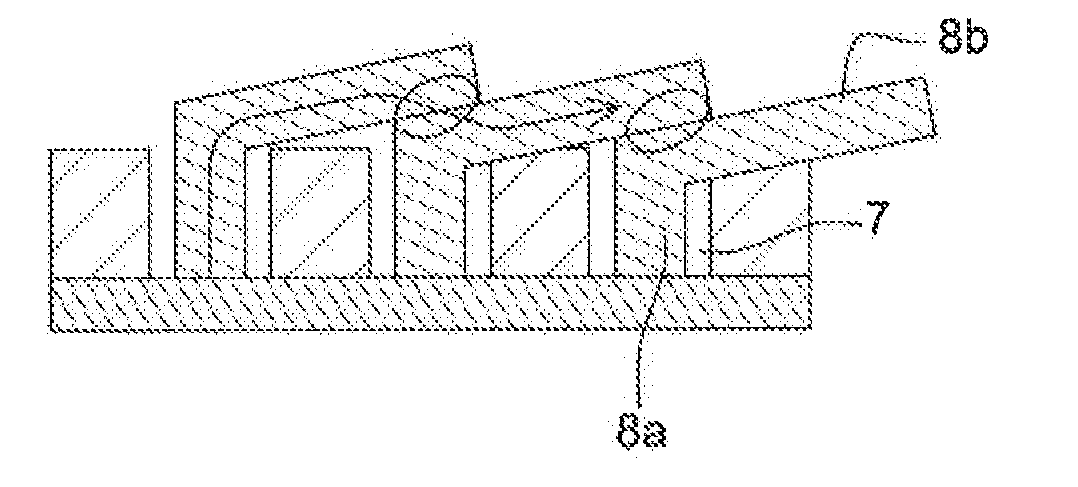
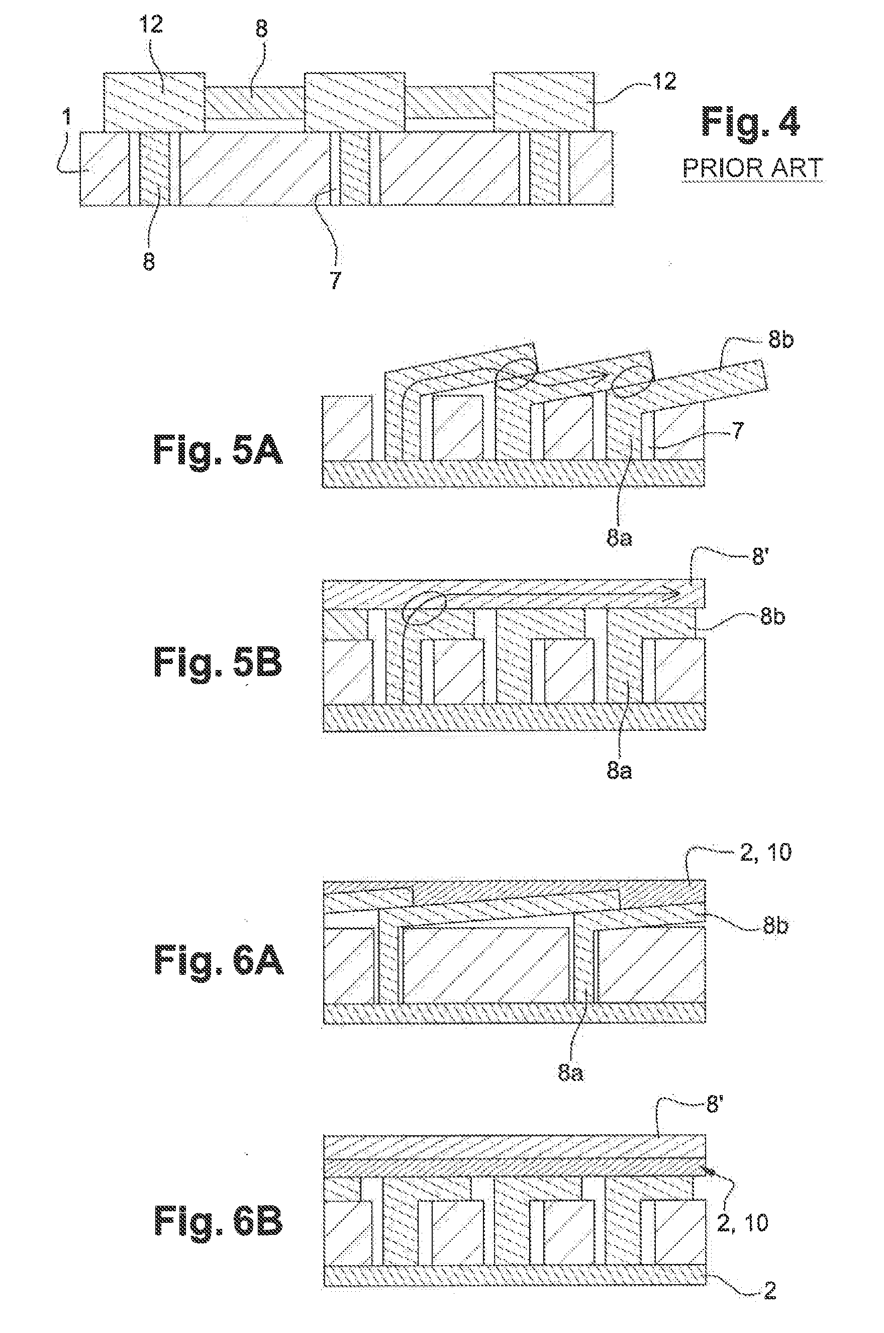
[0079]As already mentioned, this first embodiment by overlapping of vertical CNT bundles is illustrated in FIGS. 5A and 6A, respectively.

[0080]More specifically, its forming method is illustrated in FIG. 8. It should be noted that steps A to F are schematically shown in end views, that is, perpendicular to groove 3, FIGS. 8G and 8H corresponding to views parallel to the direction of groove 3.

[0081]A / Forming of the Base Structure:

[0082]An insulating layer 1, made of silica or of a low-K material of microelectronics is deposited on conductive layer 2. Conductor 2 typically is aluminum.

[0083]B / Etching of the Groove:

[0084]Within insulator 1, groove 3, which will become future line 4, is formed by conventional lithography methods.

[0085]C / TiN Deposition:

[0086]A TiN layer 5, having a thickness of approximately 50 nanometers, is deposited in groove 3, if possible by means of a conformal deposition method. TiN has the function of inhibiting the growth o...

second embodiment

II / Second Embodiment of the Invention

[0105]This second embodiment is illustrated in FIGS. 5B, 6B, 7, 9, and 10,

[0106]FIG. 5B illustrates the fact that the line resistance is lower than in the first embodiment since there is only one interface resistance left.

[0107]FIG. 7 is a drawing illustrating the principle of this second embodiment according to which the substantially perpendicular interconnects, respectively vias 7 and lines 4, come from at least two different bundles of nanotubes, advantageously formed simultaneously. It should be noted that the diagrams of the left-hand portion show cross-section views while the right-hand diagrams are top views.

[0108]Further, the embodiment implying the simultaneous growth of nanotubes 8 and 8′ from line 4 and vias 7 is illustrated in FIG. 9, which is derived from FIG. 8.

[0109]Steps A to C are similar to those of FIG. 8.

[0110]However, before the opening of vias 7, an additional step is carried out (FIG. 9D′): an opening 9 of TiN 5 is formed...


PUM

PropertyMeasurementUnit
thicknessaaaaaaaaaa
pressureaaaaaaaaaa
electric resistanceaaaaaaaaaa

Abstract

The invention relates to an electronic device including electric connections extending along at least two different directions, said connections being essentially formed by means of bundles of carbon nanotubes (CNT) (8), where at least two CNT bundles comprise a portion (8a) having its axis directed along a first direction and a portion (8b) having its axis redirected along a second direction, the connections between CNT bundles being achieved by overlapping of the portions (8b) of said at least two bundles to form a connection line (4).

Description

TECHNICAL FIELD[0001]The present disclosure relates to an electronic device comprising electric connections formed by means of carbon nanotubes (CNT), it also relates to methods for forming such connections.[0002]This invention especially has applications for thermal, electric, and mechanical connectors.BACKGROUND OF THE INVENTION[0003]The use of carbon nanotubes (CNT) or of CNT bundles to manufacture through vias or chip interconnects has already been provided, especially to provide a complement or even an alternative to the use of copper, indeed, the latter is not adapted when minute sizes are involved, CNTs further have the necessary properties, such as a low electric resistance, enabling to provide the best electric conductivity between the different chip levels.[0004]A via is a cavity enabling to create a connection between conductive plates. The electric lines formed on the plates create the connection between vias. Conductive plates are made of a metal, such as aluminum, and ...

Claims


Application Information

Patent Timeline
Patent Type & Authority Applications(United States)
IPC IPC(8): H02G15/08H05K13/00B82Y99/00
CPCH01L21/76877H01L23/53276H01L2221/1094H01L2924/0002Y10S977/842Y10T29/49002B82Y40/00H01L21/76841Y10T29/49117H01L2924/00H01L24/19H01L24/20H01L2224/215
Inventor DIJON, JEAN
Owner COMMISSARIAT A LENERGIE ATOMIQUE ET AUX ENERGIES ALTERNATIVES
Why Eureka
Try Eureka