Ferroelectric semiconductor transistor devices having gate modulated conductive layer

a technology of ferroelectric semiconductor and gate modulation, which is applied in the direction of semiconductor devices, basic electric elements, electrical equipment, etc., can solve the problems of fundamental lower operating voltage limit of conventional fet semiconductor switches and difficulty in lowering supply voltag

Active Publication Date: 2012-11-22
IBM CORP
View PDF9 Cites 34 Cited by
  • Summary
  • Abstract
  • Description
  • Claims
  • Application Information

AI Technical Summary

Benefits of technology

[0003]Exemplary embodiments of the invention generally include semiconductor switching devices and more specifically, field effect transistor (FET) devices having gate stack structures formed with a ferroelectric layer disposed between a gate contact and a thin conductive layer (“quantum conductive layer”) . The gate contact and ferroelectric layer serve to modulate an effective work function of the thin conductive layer. The thin conductive layer with the modulated work function is coupled to a semiconductor channel layer to modulate current flow through the semiconductor and achieve a steep sub-threshold slope substantially lower than 60 mV / decade.

Problems solved by technology

One of the main barriers to achieving lower energy CMOS (complementary metal oxide semiconductor) logic is the difficulty in lowering the supply voltage.
This minimum sub-threshold slope results in a fundamental lower limit on the operating voltage for conventional FET semiconductor switches.

Method used


Image

  • Ferroelectric semiconductor transistor devices having gate modulated conductive layer
  • Ferroelectric semiconductor transistor devices having gate modulated conductive layer
  • Ferroelectric semiconductor transistor devices having gate modulated conductive layer

Examples


Embodiment Construction

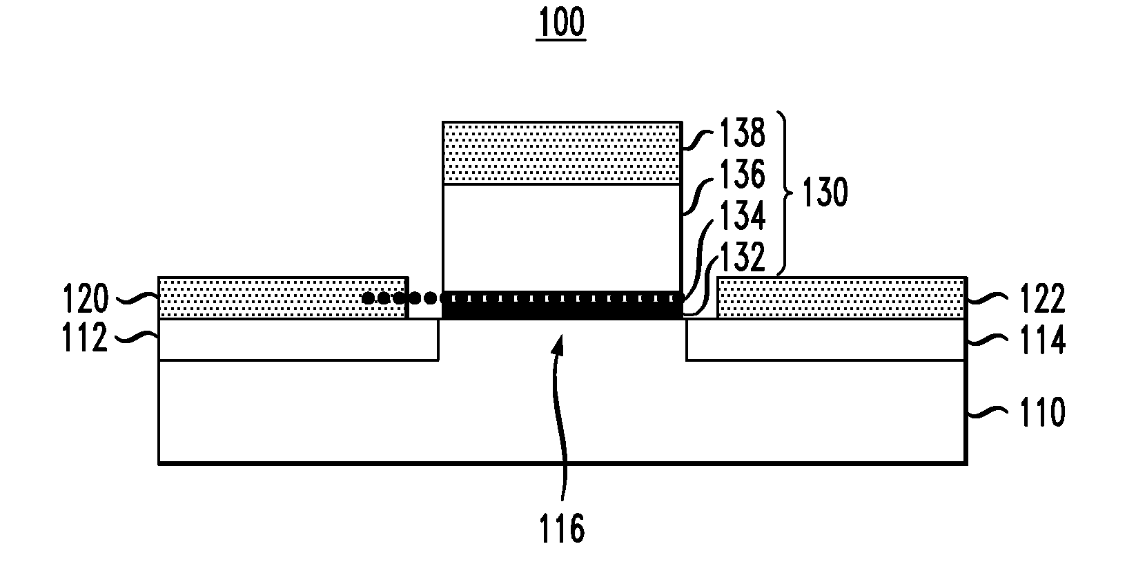
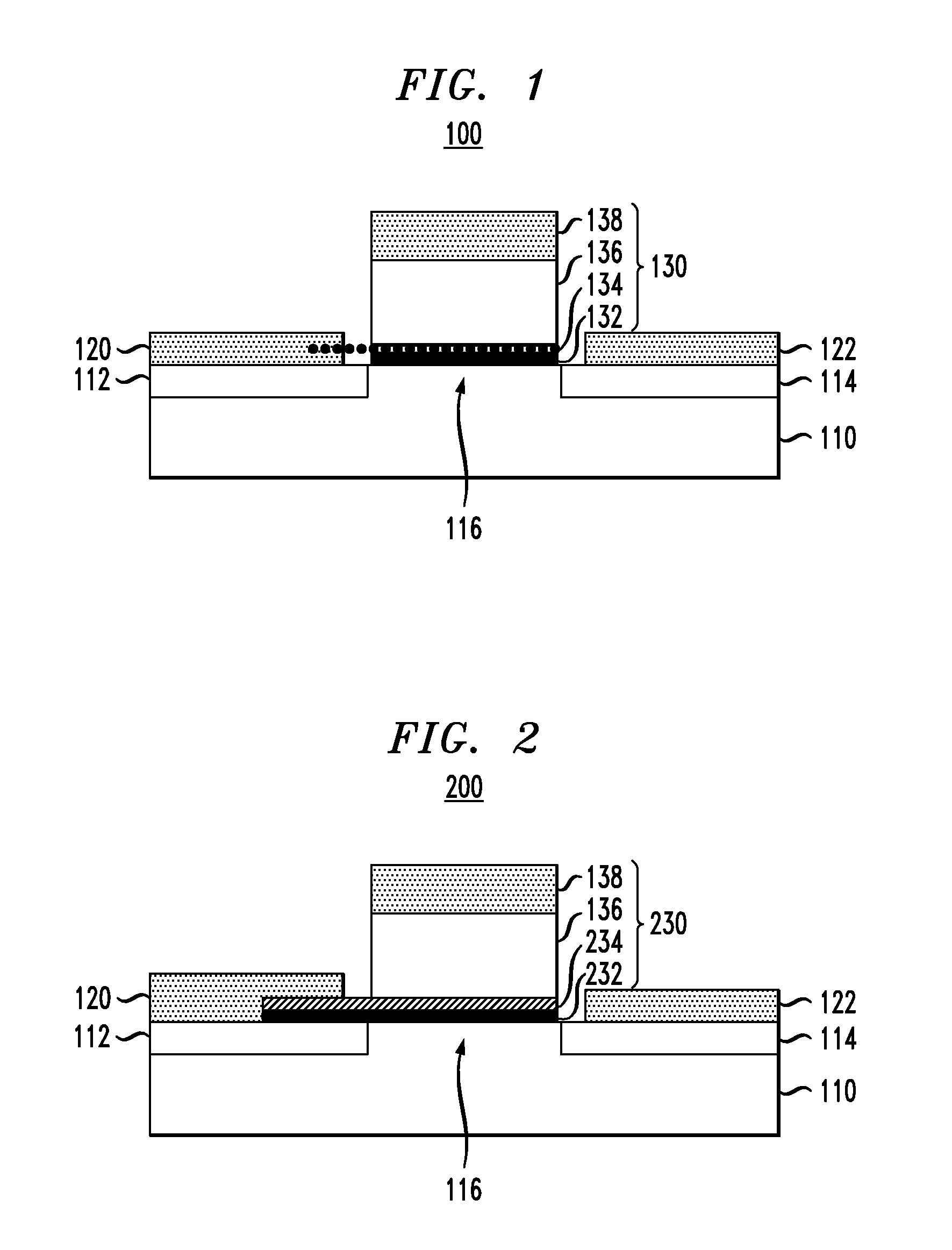
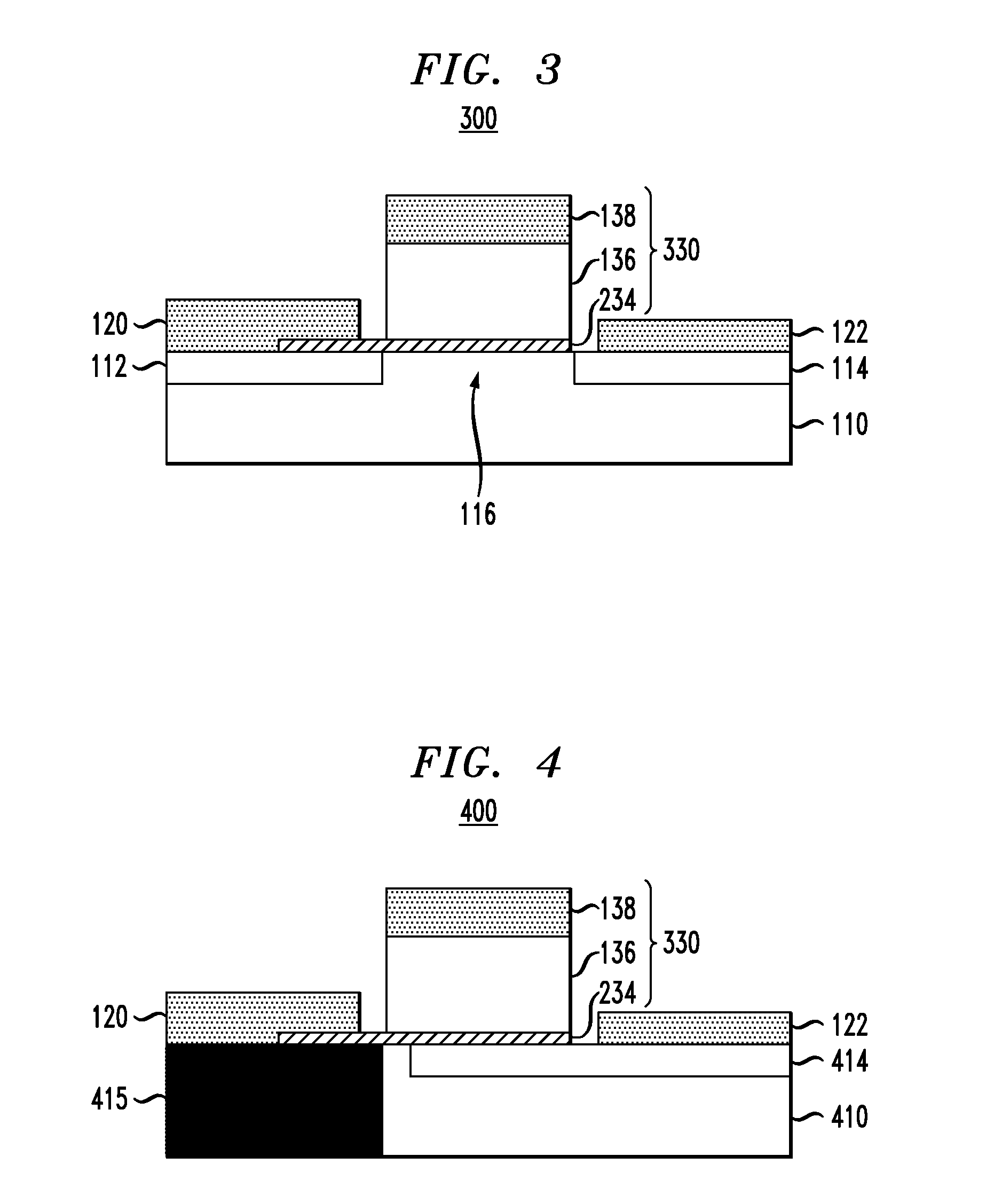
[0018]Exemplary embodiments of the invention will now be described in further detail with reference to ferroelectric semiconductor switching devices and, more specifically, field effect transistor (FET) devices having gate stack structures formed with a ferroelectric layer disposed between a gate contact and a thin conductive or metal layer (referred to herein as “quantum conductive layer”) . The gate contact and ferroelectric layer serve to modulate an effective work function of the quantum conductive layer. The quantum conductive layer with the modulated work function is coupled to a semiconductor channel layer to modulate current flow through the semiconductor and achieve a steep sub-threshold slope.

[0019]Recently, it was suggested that gate dielectrics containing a ferroelectric (FE) layer could enable the fabrication of MOSFETs with steep sub-threshold slope, exceeding the conventional limit of 60 mV / decade. See Salahuddin, et al., “Use of Negative Capacitance to Provide Voltag...


PUM


Abstract

Ferroelectric semiconductor switching devices are provided, including field effect transistor (FET) devices having gate stack structures formed with a ferroelectric layer disposed between a gate contact and a thin conductive layer (“quantum conductive layer”) . The gate contact and ferroelectric layer serve to modulate an effective work function of the thin conductive layer. The thin conductive layer with the modulated work function is coupled to a semiconductor channel layer to modulate current flow through the semiconductor and achieve a steep sub-threshold slope.

Description

TECHNICAL FIELD[0001]This invention relates generally to semiconductor switching devices and, in particular to ferroelectric semiconductor field effect transistor (FET) devices having gate stack structures formed with a ferroelectric layer that couples a gate contact to a thin conductive layer to modulate an effective work function of the thin conductive layer and, in turn, modulate current flow through a semiconductor channel and achieve a steep sub-threshold slope.BACKGROUND[0002]One of the main barriers to achieving lower energy CMOS (complementary metal oxide semiconductor) logic is the difficulty in lowering the supply voltage. The supply voltage is constrained by the sub-threshold swing, which is limited by Fermi-Dirac statistics to 60 mV / decade at room temperature. In particular, it is known that with a conventional field effect transistor, a change in the channel potential of at least 60 mV at 300 K is needed to cause a change in the current by a factor of 10. This minimum s...

Claims


Application Information

Patent Timeline
Patent Type & Authority Applications(United States)
IPC IPC(8): H01L29/772
CPCH01L29/42316H01L29/4232H01L29/812
Inventor DUBOURDIEU, CATHERINE A.FRANK, DAVID J.FRANK, MARTIN M.NARAYANAN, VIJAYSOLOMON, PAUL M.THEIS, THOMAS N.
Owner IBM CORP
Why Eureka
Try Eureka