Semiconductor device

a technology semiconductor devices, applied in the direction of pulse techniques, instruments, computation using denominational number representation, etc., can solve the problems of high potential, high power consumption of electronic devices, and the need for reducing the power consumption of semiconductor integrated circuits used in electronic devices, so as to reduce power consumption and reduce cost. , the effect of increasing the design flexibility

Inactive Publication Date: 2012-11-22
SEMICON ENERGY LAB CO LTD
View PDF4 Cites 32 Cited by
  • Summary
  • Abstract
  • Description
  • Claims
  • Application Information

AI Technical Summary

Benefits of technology

[0014]Although a programmable circuit including an analog circuit (analog element) has not yet been widely used as compared to a programmable logic device including a digital circuit, development of the programmable circuit has been desired for circuit space-saving, a reduction in cost, and an increase in design flexibility.
[0015]In view of the above problems, an object of an embodiment of the present invention is to provide a programmable analog device with which data can be held even while supply of a power supply potential is stopped and with which power consumption can be reduced.

Problems solved by technology

In recent years, the reduction in power consumption of electronic devices is an important issue, and lower power consumption of semiconductor integrated circuits used in electronic devices is also strongly required.
However, since electrons are injected into a floating gate to write data, there are problems in that a high potential is required and it takes a long time to write data.
Moreover, tunneling current generated in data writing causes deterioration of a gate insulating layer of a floating gate.
Further, a floating gate transistor has low data write / read speed and is thus unsuitable for intermittent operation.

Method used


Image

  • Semiconductor device
  • Semiconductor device
  • Semiconductor device

Examples


embodiment 1

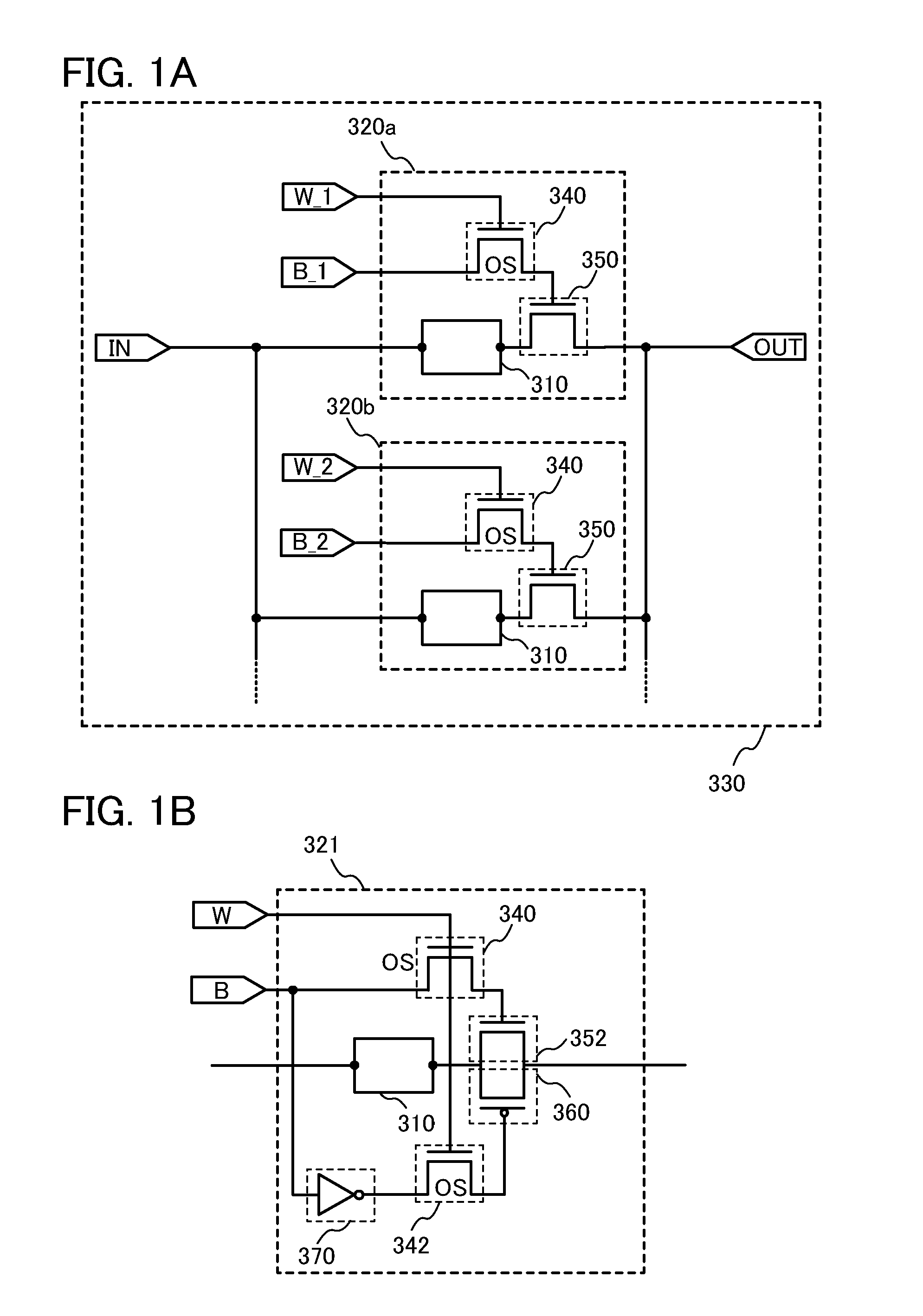
[0055]In this embodiment, a circuit configuration of a semiconductor device according to an embodiment of the disclosed invention will be described with reference to FIGS. 1A and 1B and FIGS. 2A and 2B.

1>

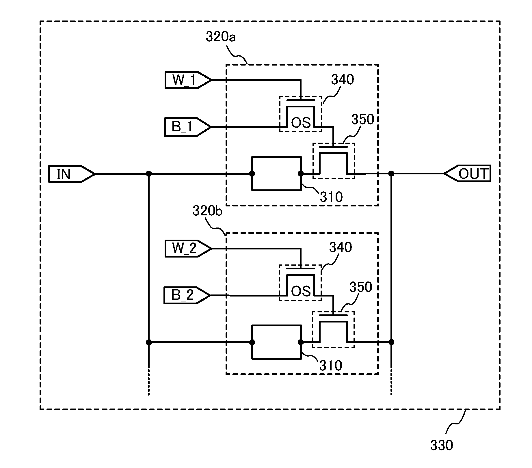
[0056]FIG. 1A illustrates a configuration of a programmable circuit 330 in this embodiment. The programmable circuit 330 includes a plurality of unit cells connected in parallel between an input signal line IN and an output signal line OUT. In FIG. 1A, a unit cell 320a and a unit cell 320b are connected in parallel. Note that an embodiment of the present invention is not limited to this configuration, and three or more unit cells may be connected in parallel.

[0057]The unit cells 320 (unit cell 320a and unit cell 320b) are electrically connected to bit lines B (bit line B_1 and bit line B_2) and word lines W (word line W_1 and word line W_2). In FIG. 1A, the unit cell 320a is electrically connected to the word line W_1 and the bit line B_1, and the unit cell 320b is electrically conn...

embodiment 2

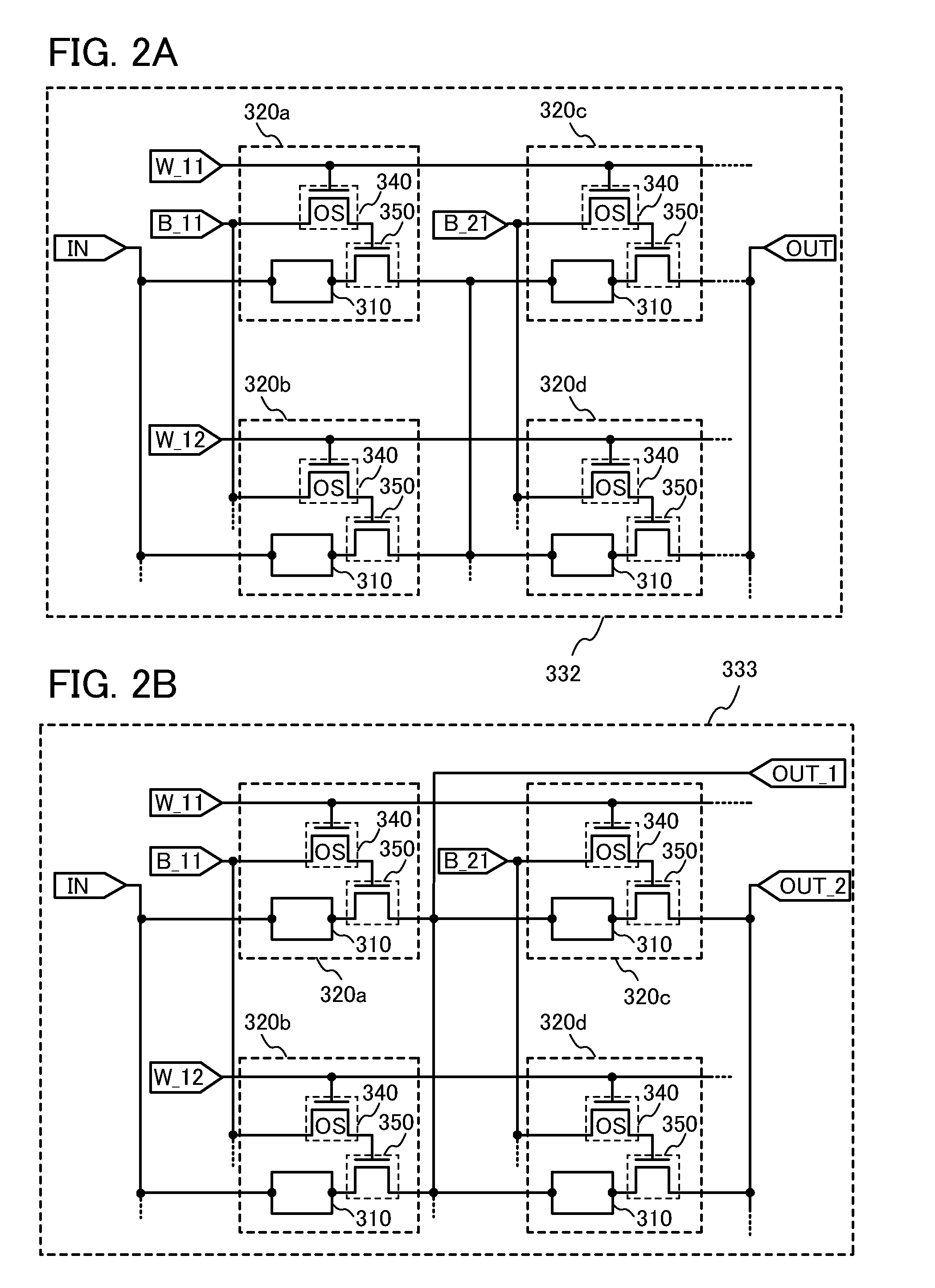
[0080]In this embodiment, an application example of the programmable circuit 330 in Embodiment 1 will be described. Needless to say, an analog element described in this embodiment can be applied to the programmable circuit 332. Further, an analog element other than that described in this embodiment can be applied to the programmable circuit according to one embodiment of the present invention.

application example 1

[0081]FIG. 3A illustrates a programmable circuit 334 in which a capacitor 312 is used as the analog element 310 in the programmable circuit 330 illustrated in FIG. 1A.

[0082]The programmable circuit 334 includes a unit cell 322a and a unit cell 322b connected in parallel between an input signal line IN and an output signal line OUT. The unit cells 322 (unit cell 322a and unit cell 322b) each include the capacitor 312 which corresponds to the analog element 310 in the unit cell 320 in FIG. 1A. One of electrodes of the capacitor 312 is electrically connected to the input signal line IN, and the other of the electrodes of the capacitor 312 is electrically connected to one of source and drain electrodes of a second transistor 350. The structure of each of the unit cells 322 is the same as that of the unit cell 320 expect for the capacitor 312.

[0083]The capacitance value output from the programmable circuit 334 illustrated in FIG. 3A can be changed by controlling the potential of the gate...


PUM


Abstract

A programmable analog device in which data can be held even when supply of a power supply potential is stopped. The programmable circuit includes unit cells connected in parallel or in series, and each of the unit cells includes an analog element. A conduction state of each of the unit cells is changed between an on state and an off state. Each of the unit cells includes, as a switch of the unit cell, a first transistor having a sufficiently low off-state current and a second transistor, a gate electrode of the second transistor being electrically connected to a source or drain electrode of the first transistor. The conduction state of the unit cell is controlled with a potential of the gate electrode of the second transistor, which can be kept even when no power is supplied thanks to the low off-state current of the first transistor.

Description

BACKGROUND OF THE INVENTION[0001]1. Field of the Invention[0002]The invention disclosed in this specification relates to semiconductor devices.[0003]Note that a semiconductor device in this specification and the like refers to any devices that can function by utilizing semiconductor characteristics, and semiconductor elements, electro-optical devices, storage devices, signal processing units, semiconductor circuits, and electronic devices are all semiconductor devices.[0004]2. Description of the Related Art[0005]The configurations of semiconductor integrated circuits typified by LSIs are fixed at the time of manufacture and cannot be generally changed after manufacture. In contrast, in semiconductor integrated circuits called programmable logic devices (PLDs), considering a logic unit composed of a plurality of logic circuits as a unit, logic units are electrically connected through wirings. In a programmable logic device, the circuit configuration of each logic unit can be electric...

Claims


Application Information

Patent Timeline
Patent Type & Authority Applications(United States)
IPC IPC(8): H03K19/177
CPCH03K19/1776H01L27/105H03K19/17772H03K19/17764H10B63/80H10B63/30G11C16/10
Inventor OHMARU, TAKUROSHIONOIRI, YUTAKA
Owner SEMICON ENERGY LAB CO LTD
Why Eureka
Try Eureka