Display substrate, method of manufacturing the same and display panel having the same

a technology of display substrate and manufacturing method, which is applied in the direction of liquid/solution decomposition chemical coating, superimposed coating process, instruments, etc., can solve the problems of static friction and the reduction of the yield of manufacturing the display apparatus

Active Publication Date: 2012-11-22
SAMSUNG DISPLAY CO LTD
View PDF2 Cites 13 Cited by
  • Summary
  • Abstract
  • Description
  • Claims
  • Application Information

AI Technical Summary

Benefits of technology

[0032]According to the example embodiments, a plurality of sub-concave portions having depths different from each other are Ruined on the micro shutter, so that a static friction between the base substrate and the micro shutter spaced apart and floated from the base substrate may be decreased.

Problems solved by technology

However, a static friction occurs due to a molecular force of molecules on a contact surface between the DMS and the backplane.
As a result, the second substrate may be damaged and a yield of manufacturing the display apparatus may be decreased.

Method used


Image

  • Display substrate, method of manufacturing the same and display panel having the same
  • Display substrate, method of manufacturing the same and display panel having the same
  • Display substrate, method of manufacturing the same and display panel having the same

Examples


Embodiment Construction

[0042]Hereinafter, embodiments of the present invention will be explained in detail with reference to the accompanying drawings.

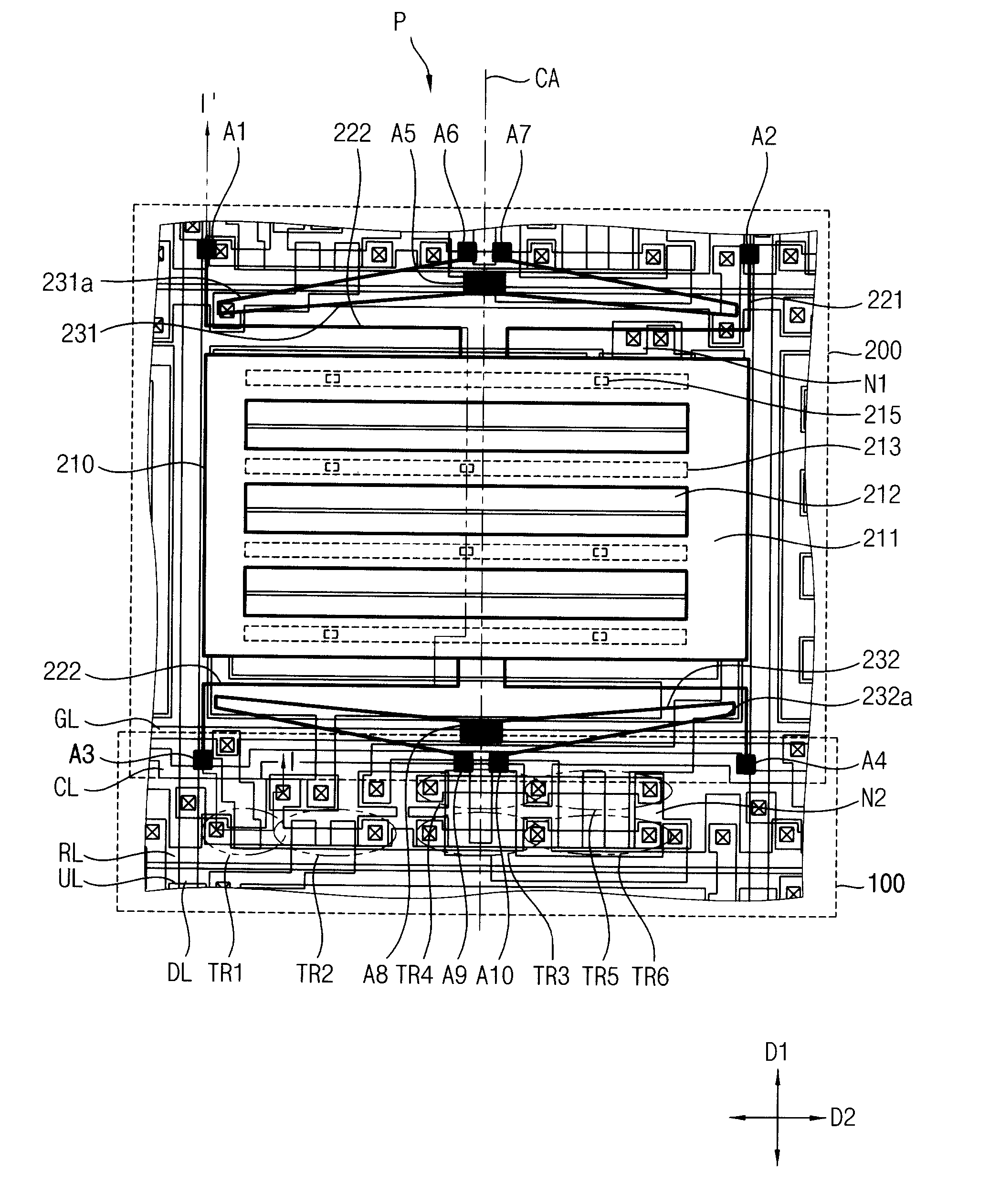
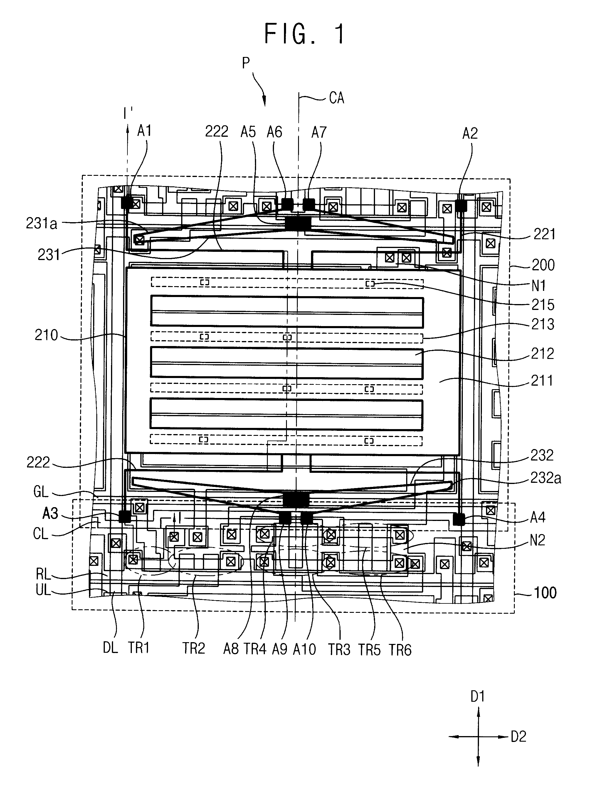
[0043]FIG. 1 is a plan view illustrating a portion of a display panel according to an example embodiment of the present invention.

[0044]Referring to FIG. 1, the display panel includes a plurality of pixels, and each pixel P includes a circuit part 100 and a shutter part 200.

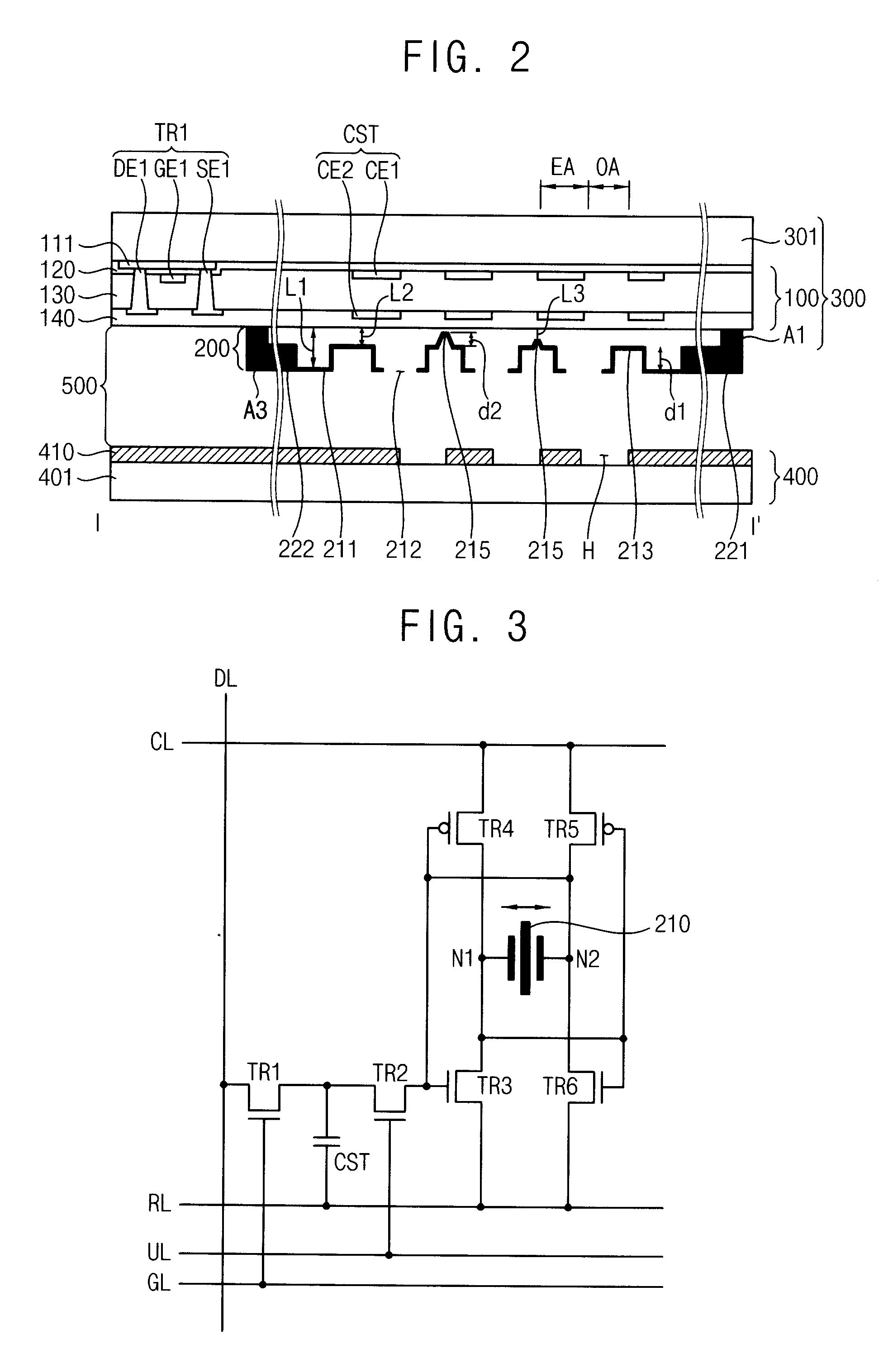
[0045]The circuit part 100 includes a plurality of signal lines DL, GL, CL, RL and UL, a plurality of transistors TR1, TR2, TR3, TR4, TR5 and TR6, and a storage capacitor CST (see FIG. 2). The circuit part 100 is electrically connected to the shutter part 200 to control the shutter part 200.

[0046]The shutter part 200 includes a micro shutter 210, a plurality of driving electrodes 221 and 222, a plurality of reference electrodes 231 and 232, and a plurality of anchors A1, A2, . . . , A10.

[0047]The micro shutter 210 includes a flat portion 211, at least one opening 212 formed on the flat p...


PUM

PropertyMeasurementUnit
depthaaaaaaaaaa
depthsaaaaaaaaaa
cone shapeaaaaaaaaaa

Abstract

A display substrate includes a base substrate, a micro shutter, a first driving electrode, a second driving electrode, and a plurality of anchors. The micro shutter includes a flat portion having at least one opening, a main concave portion adjacent to the opening and extending in from the flat portion to a first depth, and at least one sub-concave portion extending in from a bottom surface of the main concave portion to second depth. The first driving electrode is connected to a first side of the micro shutter. The second driving electrode is connected to a second side of the micro shutter. The second side is positioned opposite to the first side. The anchors fix the first and second driving electrodes on the base substrate.

Description

CROSS-REFERENCE TO RELATED APPLICATION[0001]This application claims priority under 35 U.S.C. §119 to Korean Patent Application No. 2011-47401, filed on May 19, 2011, in the Korean Intellectual Property Office (KIPO), the contents of which are herein incorporated by reference in their entireties.BACKGROUND OF THE INVENTION[0002]1. Technical Field[0003]Example embodiments of the present invention relate to a display substrate, a method of manufacturing the display substrate and a display panel having the display substrate. More particularly, example embodiments of the present invention relate to a display substrate having a digital micro shutter (DMS), a method of manufacturing the display substrate and a display panel having the display substrate.[0004]2. Discussion of the Related Art[0005]Generally, a display apparatus displays an image or data inputted by an input device. For example, a cathode ray tube, a liquid crystal display (LCD), a plasma display panel (PDP) and a field emiss...

Claims


Application Information

Patent Timeline
Patent Type & Authority Applications(United States)
IPC IPC(8): G02B26/02H05K3/02H01L33/08
CPCG02B26/023G02F1/133G02F1/1333G02F1/1335G02F1/1343
Inventor CHO, HYUN-MINYUN, SUNG-SIKPARK, JAE-BYUNGCHO, DON-CHANKIM, DAE-HYUNYOON, SEON-TAE
Owner SAMSUNG DISPLAY CO LTD
Why Eureka
Try Eureka