Method for fabricating micro-mechanical devices

a micro-mechanical device and gyroscope technology, applied in the field of forming gyroscopes and accelerometers, can solve the problems of limiting the thickness of the resulting device, non-uniform stress gradient, structure bending, etc., and achieves thicker micro-mechanical structures, reduces stiction, and eliminates or minimizes the need for highly corrosive wet chemical etches

Active Publication Date: 2007-11-27
CHARLES STARK DRAPER LABORATORY
View PDF26 Cites 13 Cited by
  • Summary
  • Abstract
  • Description
  • Claims
  • Application Information

AI Technical Summary

Benefits of technology

[0011]It is a further object of this invention to provide such a method which reduces dislocation caused by lattice mismatch.
[0012]It is a further object of this invention to provide such a method which is lower in cost.
[0014]It is a further object of this invention to provide such a method which reduces stiction.
[0015]It is a further object of this invention to provide such a method which eliminates or minimizes the need for highly corrosive wet chemical etches.
[0016]It is a further object of this invention to provide to such a method which results in thicker micro-mechanical structures that can be used to increase the mass and horizontal motion stiffness of micro-mechanical gyroscopes and accelerometer designs.

Problems solved by technology

The use of boron as an etch stop layer, however, may limit the thickness of the resulting device because boron diffusion is currently limited to a thickness of approximately 20 μm.
The boron doping gradient generated by the diffusion process also creates a non-uniform stress gradient through the thickness of the micro-mechanical structure which has been shown to cause the structures to bend.
Heavily boron doped silicon produced by diffusion is known to have a high density of dislocations caused by lattice mismatch of the boron doped layer with the undoped silicon substrate.
Deposition of thick boron doped epitaxial layers is also expensive.
Heavily boron doped epitaxial layers have been demonstrated with a thickness of up to 50 μm but at a high cost (e.g., epitaxy cost can exceed $300.00 per wafer).
Epitaxy costs are expected to increase as the thickness is increased.
If germanium is used to lower the stress, the result is a low mechanical quality factor which is disadvantageous in many applications such as vibrating angular rate sensors and resonators.
If features such as access ports are present, wet chemical etches cannot typically be used.
In addition, the EDP etch required to dissolve the undoped portions of the silicon wafer is a highly corrosive wet chemical etch necessitating special exhaust and chemical handling procedures.
Finally, sticking is a major failure mode for devices fabricated by the dissolved wafer process.

Method used


Image

  • Method for fabricating micro-mechanical devices
  • Method for fabricating micro-mechanical devices
  • Method for fabricating micro-mechanical devices

Examples


Embodiment Construction

[0031]Aside from the preferred embodiment or embodiments disclosed below, this invention is capable of other embodiments and of being practiced or being carried out in various ways. Thus, it is to be understood that the invention is not limited in its application to the details of construction and the arrangements of components set forth in the following description or illustrated in the drawings. If only one embodiment is described herein, the claims hereof are not to be limited to that embodiment. Moreover, the claims hereof are not to be read restrictively unless there is clear and convincing evidence manifesting a certain exclusion, restriction, or disclaimer.

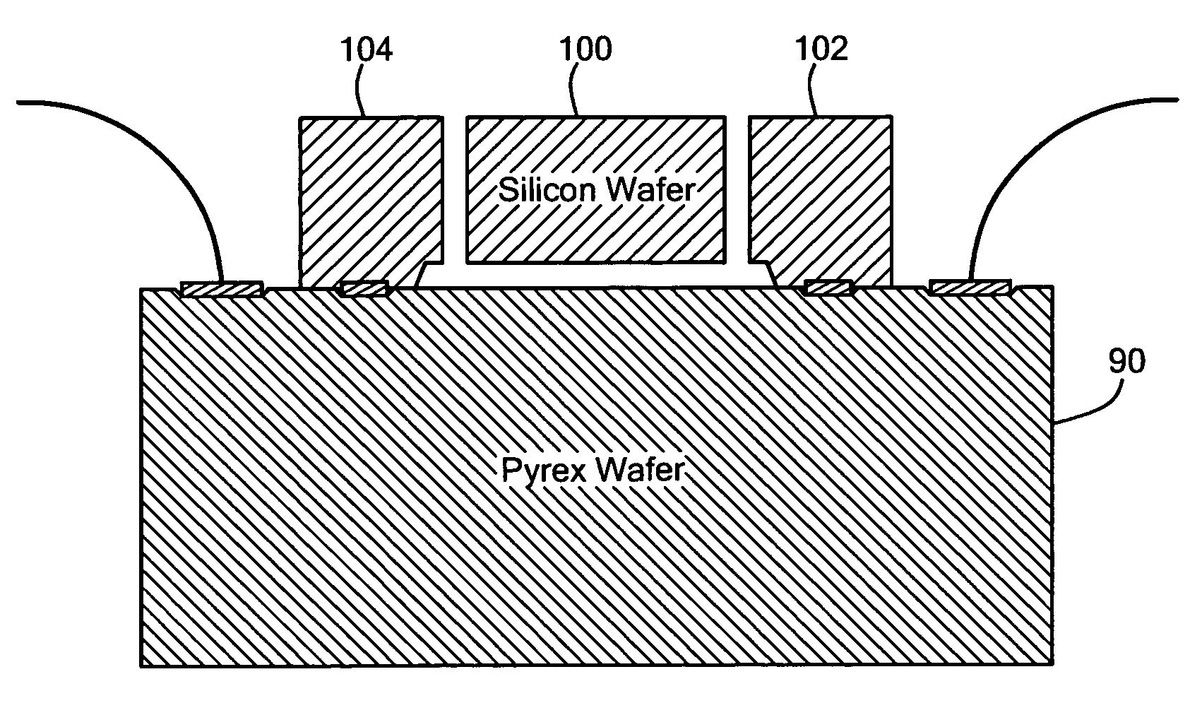
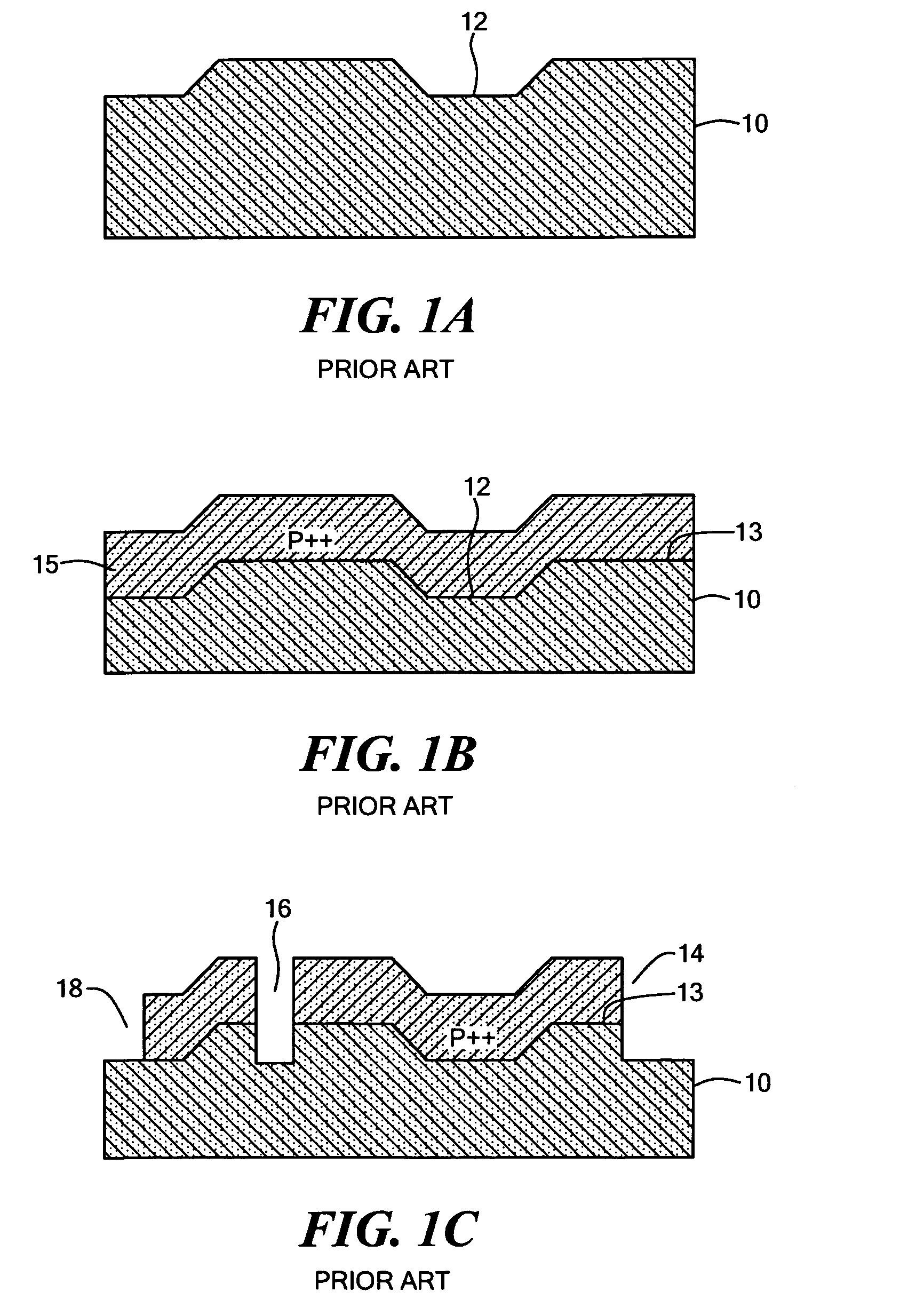
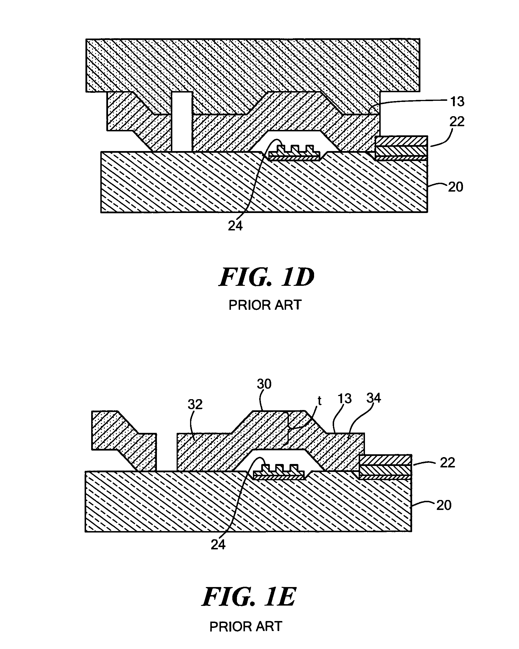
[0032]As discussed briefly in the background section above, commonly owned U.S. Pat. No. 5,492,596 discloses a method of fabricating a gyroscope or other MEMS device when silicon wafer 10, FIG. 1A is etched to form recess or mesa 12. In FIG. 1A, structure below mesa 12 will be the device structure suspended above another, t...


PUM


Abstract

A method of fabricating micro-mechanical devices. A mesa is etched in a homogeneous wafer. The wafer is bonded to a patterned substrate with the mesa defining device elements suspended above the substrate. A portion of the wafer is removed until a desired device thickness is achieved. Discrete elements of the device are then formed by performing a structural etch on the remaining wafer material.

Description

FIELD OF THE INVENTION[0001]The subject invention relates to methods of forming gyroscopes, accelerometers, and other devices including structure or structures suspended above a substrate.BACKGROUND OF THE INVENTION[0002]There are several known methods of forming gyroscopes, accelerometers, and other MEMS devices including structure suspended above a substrate.[0003]According to commonly owned U.S. Pat. No. 5,492,596, incorporated herein by this reference, a silicon wafer is etched at desired locations to define the portions of the device which are suspended above a glass substrate. Boron is then diffused into the silicon wafer to a depth which will define the thickness of the device. The glass substrate is then prepared to include electrodes and the silicon wafer, diffused with boron, is bonded to the glass substrate. Finally, the silicon substrate is thinned by etching down to the boron diffusion layer.[0004]The use of boron as an etch stop layer, however, may limit the thickness ...

Claims


Application Information

Patent Timeline
Patent Type & Authority Patents(United States)
IPC IPC(8): H01L21/00
CPCB81C3/008G01C19/5719G01P15/097G01P15/0802B81C2203/031B81B2201/0271
Inventor CUNNINGHAM, BRIAN T.WEINBERG, MARC S.
Owner CHARLES STARK DRAPER LABORATORY
Why Eureka
Try Eureka