Method of Manufacturing Light-Emitting Device and Light-Emitting Device

a technology of light-emitting devices and manufacturing methods, which is applied in the direction of organic semiconductor devices, solid-state devices, thermoelectric devices, etc., can solve the problems of thermal or physical damage to the light-emitting element, the problem of affecting the light-emitting element, and the visible gradient of the luminance, so as to achieve high-reliable light-emitting devices, prevent metal mask problems, and ensure the effect of light-emitting devices

Inactive Publication Date: 2012-11-29
SEMICON ENERGY LAB CO LTD
View PDF5 Cites 16 Cited by
  • Summary
  • Abstract
  • Description
  • Claims
  • Application Information

AI Technical Summary

Benefits of technology

[0008]Meanwhile, as for formation of a light-emitting element, as an example of a method of stacking a layer containing a light-emitting organic compound and an upper electrode layer in this order over a lower electrode layer formed over a substrate having an insulating surface, a vacuum evaporation method is given. As a method of forming an island-shaped layer by a vacuum evaporation method, a method using a metal mask (also referred to as a shadow mask), which is a metal plate provided with an opening, is known. The metal mask is provided between a substrate and an evaporation source to be in contact with the substrate, and evaporation is performed on the substrate through the opening in the metal mask, whereby an island-shaped pattern according to the shape of the opening can be formed. Note that as the distance between the metal mask and the substrate is shorter, it is possible to form an island-shaped layer with a clearer shape based on the opening, in other words, a shape whose periphery is less obscure.
[0035]According to one embodiment of the present invention, a method of manufacturing a highly reliable light-emitting device can be provided. More specifically, a method of manufacturing a light-emitting device in which problems due to a metal mask are prevented can be provided. Further, a method of manufacturing a light-emitting device in which a problem due to the resistance of an upper electrode layer of a light-emitting element is prevented can be provided. Further, a highly reliable light-emitting device can be provided.

Problems solved by technology

When the voltage drop is significant, there arises a problem in that luminance gradient might be seen.
However, particularly in the case of a top-emission type (including a dual-emission type) in which light emission is obtained from the substrate surface side, a pattern of the auxiliary electrode layer needs to be formed after formation of the light-emitting element; accordingly, the light-emitting element might be damaged.
For example, in the case where a conductive film which is to be the auxiliary electrode layer is formed by a sputtering method, thermal or physical damage to the light-emitting element is concerned.
Further, when the conductive film is processed by a photolithography method or the like, there arise problems of optical or thermal damage to the light-emitting element, dissolution of the light-emitting element with an organic solvent, for example, at the time of removal of a resist, and the like.
On the other hand, the probability of the occurrence of problems becomes high when the metal mask is used in contact with the substrate.
For example, a substrate surface is damaged by an edge of the opening in the metal mask in some cases.
Specifically, at the time of placing the metal mask in contact with the substrate, the metal mask might scratch the substrate surface, thereby breaking another layer which has already been fanned over the substrate.
In particular, overlap between the opening edge of the metal mask and a region near a light-emitting region might short-circuit the light-emitting element.

Method used


Image

  • Method of Manufacturing Light-Emitting Device and Light-Emitting Device
  • Method of Manufacturing Light-Emitting Device and Light-Emitting Device
  • Method of Manufacturing Light-Emitting Device and Light-Emitting Device

Examples


embodiment 1

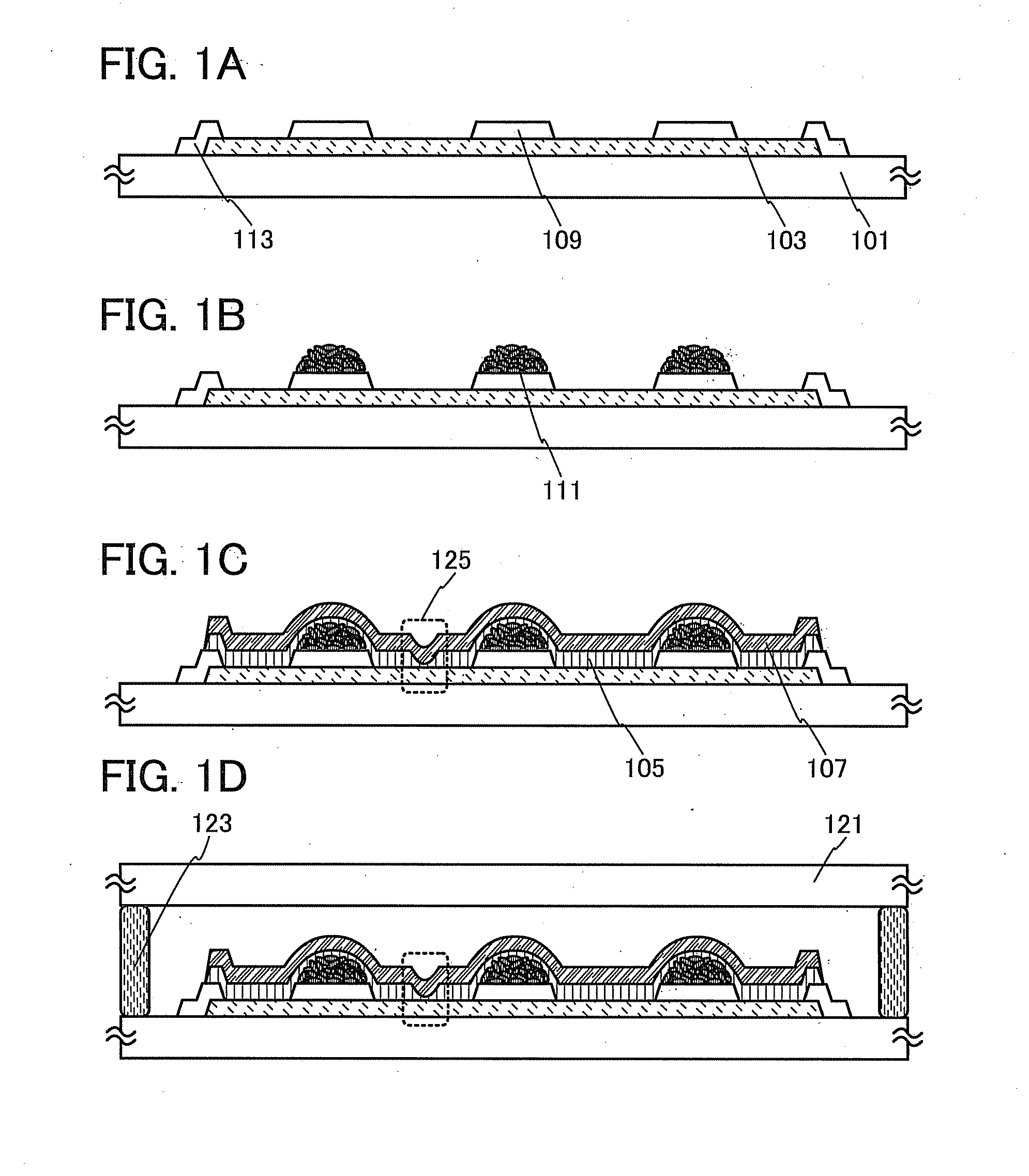
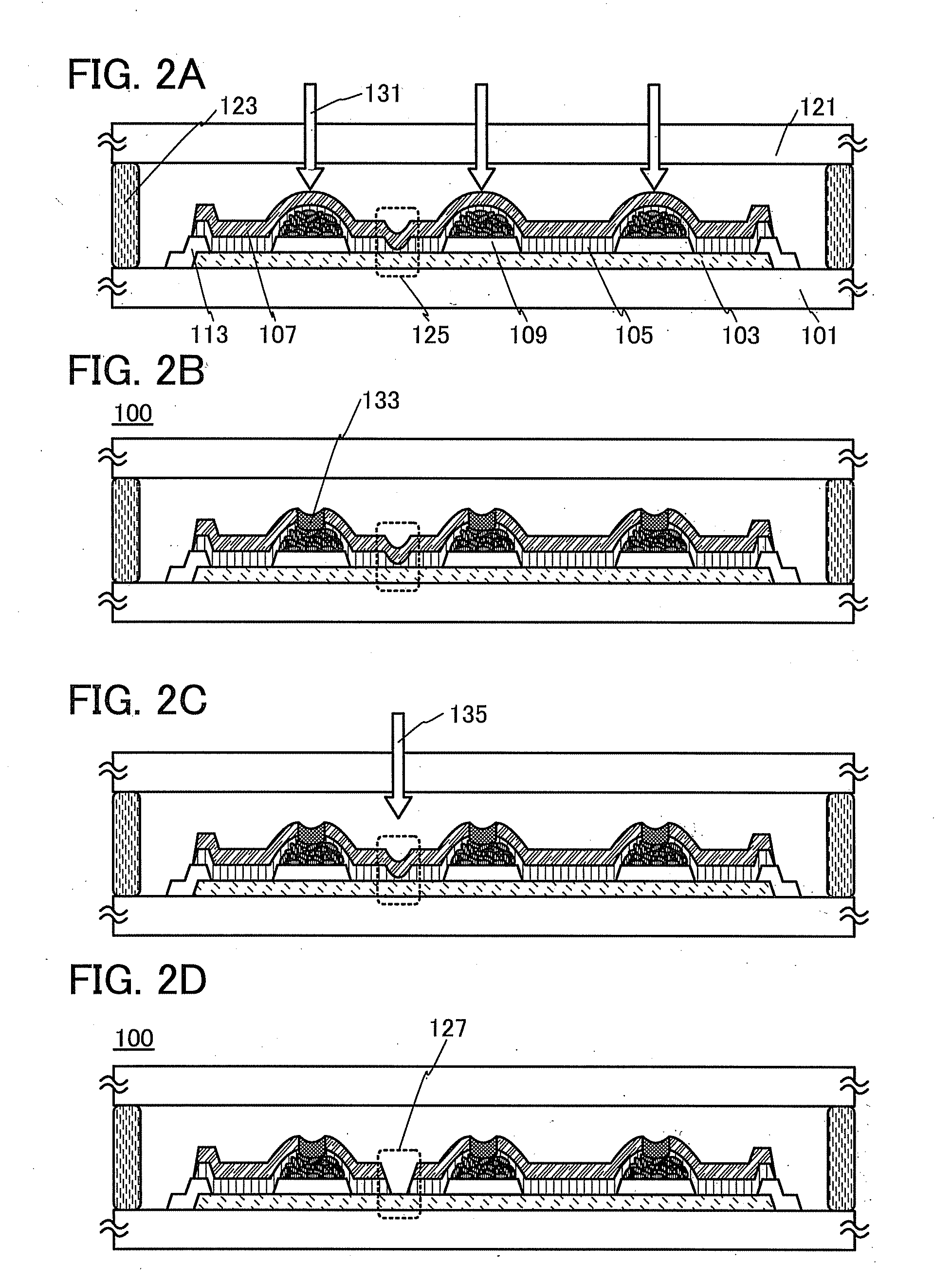
[0053]In this embodiment, an example of a method of manufacturing a light-emitting device according to one embodiment of the present invention will be described with reference to FIGS. 1A to 1D, FIGS. 2A to 2D, FIGS. 3A and 3B, FIG. 4, and FIG. 5.

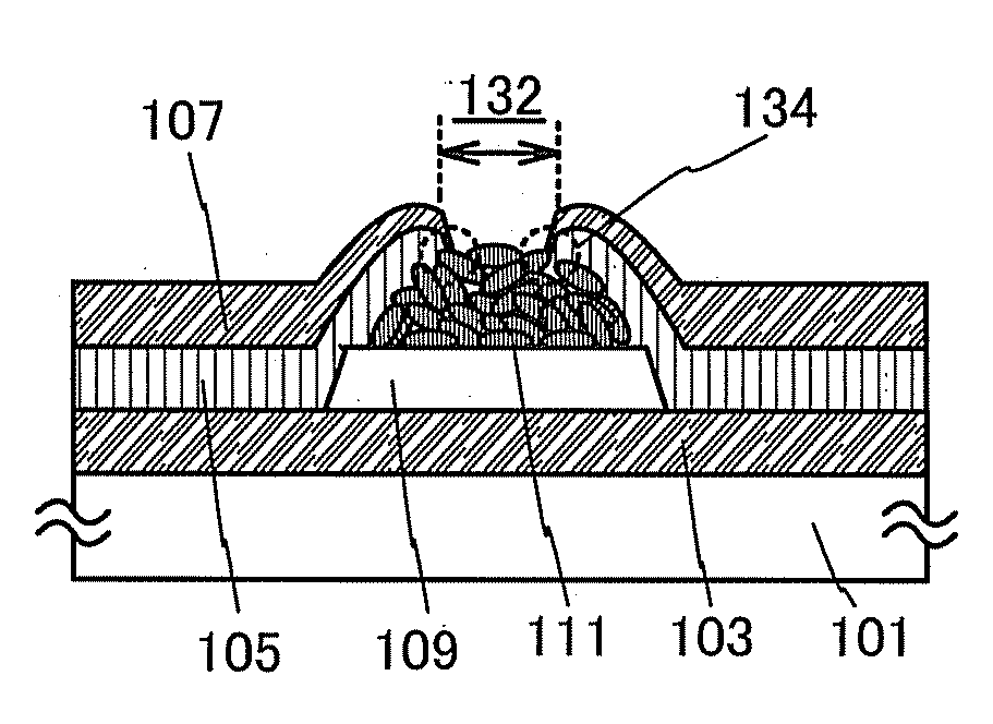
[0054]First, a substrate 101 is prepared. A lower electrode layer 103, an insulating layer 109, and an insulating layer 113 are formed over the substrate 101 (see FIG. 1A).

[0055]The lower electrode layer 103 can be Ruined in such a manner that a conductive film is formed by a film formation method such as a sputtering method, and then an unnecessary portion is removed by a patterning method such as a photolithography method.

[0056]The insulating layer 109 is provided for electrically insulating a connection electrode layer 111 formed later from the lower electrode layer 103. The insulating layer 109 can be formed by a sputtering method, a CVD method, a printing method (including a screen printing method and an offset printing method), or an ...

embodiment 2

[0144]In this embodiment, an example of a method of manufacturing a light-emitting device, which is different from that in Embodiment 1, will be described with reference to FIGS. 6A to 6D and FIG. 7. Note that the description that overlaps with that in Embodiment 1 is omitted or is simply given.

[0145]First, the lower electrode layer 103, the insulating layers 109 and 113, the connection electrode layer 111, the EL layer 105, and the upper electrode layer 107 are formed in this order over the substrate 101 as in Embodiment 1 (see FIG. 6A). Here, it is assumed that the region 125 in which the EL layer 105 is locally thin is formed.

[0146]Then, a region overlapping with the connection electrode layer 111 is irradiated with the laser light 131, so that the connection electrode layer 111 is electrically connected to the upper electrode layer 107. Irradiation with the laser light 131 may be performed by the method described in Embodiment 1.

[0147]Here, in this embodiment, a step of connecti...

embodiment 3

[0166]In this embodiment, application examples of the connection electrode layer described in the above embodiments will be described with reference to FIGS. 8A and 8B.

1>

[0167]FIG. 8A illustrates an example in which the connection electrode layer 111 is used in a dual-emission light-emitting device.

[0168]The light-emitting device illustrated in FIG. 8A includes, over the substrate 101, a lower electrode layer 163, an auxiliary electrode layer 165, an insulating layer 167, the connection electrode layer 111 having the connection portion 133, the EL layer 105, and the upper electrode layer 107.

[0169]Here, the lower electrode layer 163 has a light-transmitting property with respect to light emitted from the EL layer 105 as in the case of the upper electrode layer 107. Therefore, light emitted from the EL layer 105 is extracted from both the substrate 101 side and the surface side of the substrate 101.

[0170]Further, the auxiliary electrode layer 165 is provided in contact with the lower...


PUM


Abstract

A highly reliable light-emitting device is provided. A light-emitting device in which problems due to a metal mask are prevented is provided. A light-emitting device in which a problem due to the resistance of an upper electrode layer of a light-emitting element is prevented is provided. An electrode layer is provided over a substrate in advance, and an EL layer and an upper electrode layer are formed in the same pattern without use of a metal mask so as to overlap with the electrode layer. After that, the electrode layer is electrically connected to the upper electrode layer. As a connection method, a laser light irradiation method, a method in which physical pressure is applied, a method in which heating is performed under the state where physical pressure is applied, or the like is used.

Description

TECHNICAL FIELD[0001]The present invention relates to a method of manufacturing a light-emitting device to which an organic EL element is applied. Further, the present invention relates to a light-emitting device to which an organic EL element is applied.BACKGROUND ART[0002]Organic EL elements have been actively researched and developed. In the fundamental structure of an organic EL element, a layer containing a light-emitting organic compound is interposed between a pair of electrodes. By applying voltage to this element, light emission from the light-emitting organic compound can be obtained.[0003]The organic EL element can be formed into a film shape; thus, a large-area element can easily be formed. Therefore, the organic EL element has a high utility value as a surface light source that can be applied to lighting or the like.[0004]For example, a lighting device using an organic EL element is disclosed in Patent Document 1.[0005]In addition, as for an organic EL element, there ar...

Claims


Application Information

Patent Timeline
Patent Type & Authority Applications(United States)
IPC IPC(8): H01L51/52H01L51/56
CPCH01L51/0021H01L2251/5361H01L51/5228H01L51/5212H10K71/60H10K50/814H10K50/824H10K50/11H10K71/611H10K71/621
Inventor ADACHI, HIROKIMOMMA, YOHEI
Owner SEMICON ENERGY LAB CO LTD
Why Eureka
Try Eureka