Method for manufacturing circuit board, method for manufacturing light-emitting device,and light-emitting device

a manufacturing method and circuit board technology, applied in the field of circuit board manufacturing, can solve the problems of low processing accuracy in the depth direction, damage to wiring or the like in the lower layer, and damage to the wiring and the like of the portion to be removed, so as to achieve high-reliability light-emitting devices, the effect of reducing damage to the electrode and reducing the damage to the display region

Active Publication Date: 2017-08-15
SEMICON ENERGY LAB CO LTD
View PDF11 Cites 2 Cited by
  • Summary
  • Abstract
  • Description
  • Claims
  • Application Information

AI Technical Summary

Benefits of technology

[0014]An object of one embodiment of the present invention is to provide a method for manufacturing a circuit board or a light-emitting device in which damage to an electrode is reduced. Another object of one embodiment of the present invention is to provide a method for manufacturing a circuit board or a light-emitting device in which damage to a display region is reduced. Another object of one embodiment of the present invention is to provide a method for manufacturing a highly reliable light-emitting device. Another object of one embodiment of the present invention is to provide a highly reliable light-emitting device.
[0015]Another object of one embodiment of the present invention is to provide a novel method for manufacturing a circuit board or a light-emitting device. Another object of one embodiment of the present invention is to provide a method for manufacturing a lightweight light-emitting device. Another object of one embodiment of the present invention is to provide a method for manufacturing a thin light-emitting device. Another object of one embodiment of the present invention is to provide a novel light-emitting device.
[0030]Another embodiment of the present invention can provide a method for manufacturing a circuit board or a light-emitting device in which damage to an electrode is reduced. Another embodiment of the present invention can provide a method for manufacturing a circuit board or a light-emitting device in which damage to a display region is reduced. Another embodiment of the present invention can provide a method for manufacturing a highly reliable light-emitting device. Another embodiment of the present invention can provide a highly reliable light-emitting device.
[0031]Another embodiment of the present invention can provide a novel method for manufacturing a circuit board or a light-emitting device. Another embodiment of the present invention can provide a method for manufacturing a lightweight light-emitting device. Another embodiment of the present invention can provide a method for manufacturing a thin light-emitting device. Another embodiment of the present invention can provide a novel light-emitting device.

Problems solved by technology

In a method in which part of a flexible substrate is removed by laser light, the laser light might transmit a portion to be removed and therefore a wiring and the like below the portion to be removed might be damaged.
In a method in which part of a flexible substrate is removed by a device using an edged tool such as a scriber or a cutting plotter, the processing accuracy in the depth direction is low, and thus a wiring or the like in a lower layer might be damaged.

Method used


Image

  • Method for manufacturing circuit board, method for manufacturing light-emitting device,and light-emitting device
  • Method for manufacturing circuit board, method for manufacturing light-emitting device,and light-emitting device
  • Method for manufacturing circuit board, method for manufacturing light-emitting device,and light-emitting device

Examples


embodiment 1

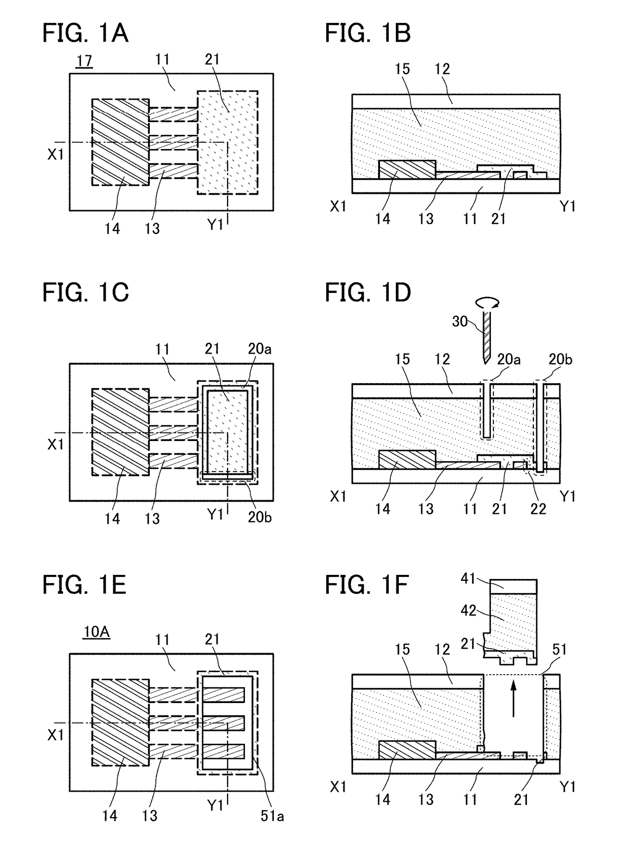
[0090]This embodiment describes structure examples of a processing member of one embodiment of the present invention and examples of a method for manufacturing a circuit board of one embodiment of the present invention with reference to FIGS. 1A to 1F, FIGS. 2A to 2F, FIGS. 3A to 3F, FIGS. 4A to 4F, FIGS. 5A to 5E, FIGS. 6A to 6F, and FIGS. 7A to 7D.

[Structure Examples of Processing Member and Examples of Method for Manufacturing Circuit Board]

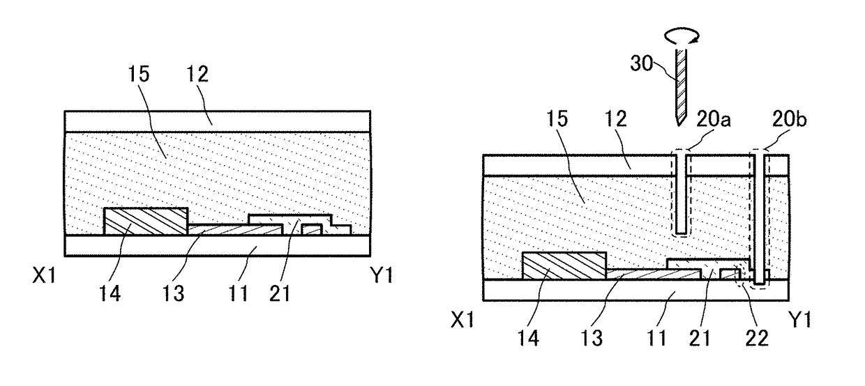
[0091]FIGS. 1A and 1B schematically illustrate a processing member of one embodiment of the present invention. FIG. 1A is a top view of a processing member 17. FIG. 1B is a cross-sectional view taken along section line X1-Y1 in FIG. 1A. FIGS. 1C to 1F illustrate an example of a method for manufacturing a circuit board of one embodiment of the present invention.

[0092]The processing member 17 includes a first substrate 11, a terminal electrode 13, a circuit 14, a bonding layer 15, a separation layer 21, and a second substrate 12. The terminal el...

modification example 1

[0120]An example of a method for manufacturing a circuit board that is different from that of the above-described circuit board 10A is described below. The above description can be referred to for the features common to the above-described example of a manufacturing method, so that the description of these features is omitted here. Only differences are described below.

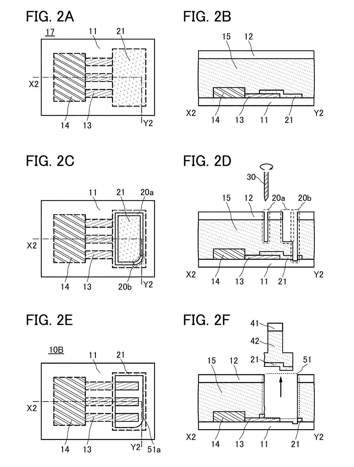
[0121]FIGS. 2A and 2B schematically illustrate a processing member of one embodiment of the present invention. FIG. 2A is a top view of a processing member 17. FIG. 2B is a cross-sectional view taken along section line X2-Y2 in FIG. 2A. The processing member 17 in FIGS. 2A and 2B has the same structure as that in FIGS. 1A and 1B except the position of the section line. An example of a method for manufacturing a circuit board of one embodiment of the present invention is described with reference to FIGS. 2C to 2F.

[0122]First, the first groove 20a and the second groove 20b are formed in the processing member 17 using a b...

modification example 2

[0128]An example of a method for manufacturing another circuit board that is formed using a processing member having a different structure from that of the processing member 17 is described below. The above description can be referred to for the features common to the above-described example of a method for manufacturing a circuit board, so that the description of these features is omitted here. Only differences are described below.

[0129]FIGS. 3A and 3B schematically illustrate a processing member of one embodiment of the present invention. FIG. 3A is a top view of a processing member 18. FIG. 3B is a cross-sectional view taken along section line X3-Y3 in FIG. 3A. FIGS. 3C to 3F illustrate an example of a method for manufacturing a circuit board of one embodiment of the present invention.

[0130]The processing member 18 differs from the processing member 17 in a region where the separation layer 21 is formed. In the processing member 17, the separation layer 21 having a rectangle shap...


PUM


Abstract

A circuit board in which damage to an electrode is reduced or a light-emitting device in which damage to an electrode is reduced is manufactured. A method for manufacturing the circuit board or the light-emitting device includes the following steps: preparing a processing member including a circuit and a terminal electrode over a first substrate, a separation layer over the terminal electrode, a bonding layer over the separation layer, and a second substrate over the bonding layer; forming a groove in the processing member using a blade capable of cutting processing by being rotated; and removing part of the separation layer, part of the bonding layer, and part of the second substrate to expose part of the terminal electrode.

Description

BACKGROUND OF THE INVENTION[0001]1. Field of the Invention[0002]One embodiment of the present invention relates to a method for manufacturing a circuit board. Another embodiment of the present invention relates to a method for manufacturing a light-emitting device. Another embodiment of the present invention relates to a light-emitting device.[0003]Note that one embodiment of the present invention is not limited to the above technical field. One embodiment of the invention disclosed in this specification and the like relates to an object, a method, or a manufacturing method. One embodiment of the present invention relates to a process, a machine, manufacture, or a composition of matter. Specifically, examples of the technical field of one embodiment of the present invention disclosed in this specification include a semiconductor device, a display device, a light-emitting device, a power storage device, a memory device, an electronic device, a lighting device, an input device, an inp...

Claims


Application Information

Patent Timeline
Patent Type & Authority Patents(United States)
IPC IPC(8): H01L27/32H01L51/56H01L51/00H05K3/00
CPCH01L27/3276H01L51/0097H01L51/56H05K3/0047H01L2227/323H01L2251/5338Y02E10/549H05K1/11H05K3/0044H05K3/0052H05K3/288H05K3/361H05K2201/09127H05K2203/0228Y02P70/50H10K59/131H10K77/111H10K59/1201H10K2102/311H10K71/00
Inventor NISHIDO, YUSUKESAKUISHI, TATSUYA
Owner SEMICON ENERGY LAB CO LTD
Why Eureka
Try Eureka