Finfet transistor structure and method for making the same

a technology of transistors and finfets, applied in the direction of transistors, semiconductor devices, electrical equipment, etc., can solve the problems of high production cost and inevitable leak current, and achieve the effect of lowering the leak current of the finfet transistor structure without reducing the heat dissipation ability of the finfet transistor structur

Active Publication Date: 2012-11-29
UNITED MICROELECTRONICS CORP
View PDF2 Cites 57 Cited by
  • Summary
  • Abstract
  • Description
  • Claims
  • Application Information

AI Technical Summary

Benefits of technology

[0008]The present invention accordingly proposes a method for forming various FINFET transistor structures to obtain various FINFET transistor structures to meet various demands. The present invention utilizes the different possibilities for forming oxide to construct FINFET transistors of different structures. In one aspect, there is no need to use the expensive SOI substrate and a FINFET transistor structure disposed on an insulating layer ...

Problems solved by technology

However, as the critical dimension of the devices shrinks, in particular for the generations after 65 nm, the multi-gate devices such as a fin field effect transistor (FinFET) is proposed to replace the planar complementary MOS since it is getting harder and harder to reduce the physical dimension of the conventional planar complementary MOS.
However, in one aspect, because som...

Method used


Image

  • Finfet transistor structure and method for making the same
  • Finfet transistor structure and method for making the same
  • Finfet transistor structure and method for making the same

Examples


first embodiment

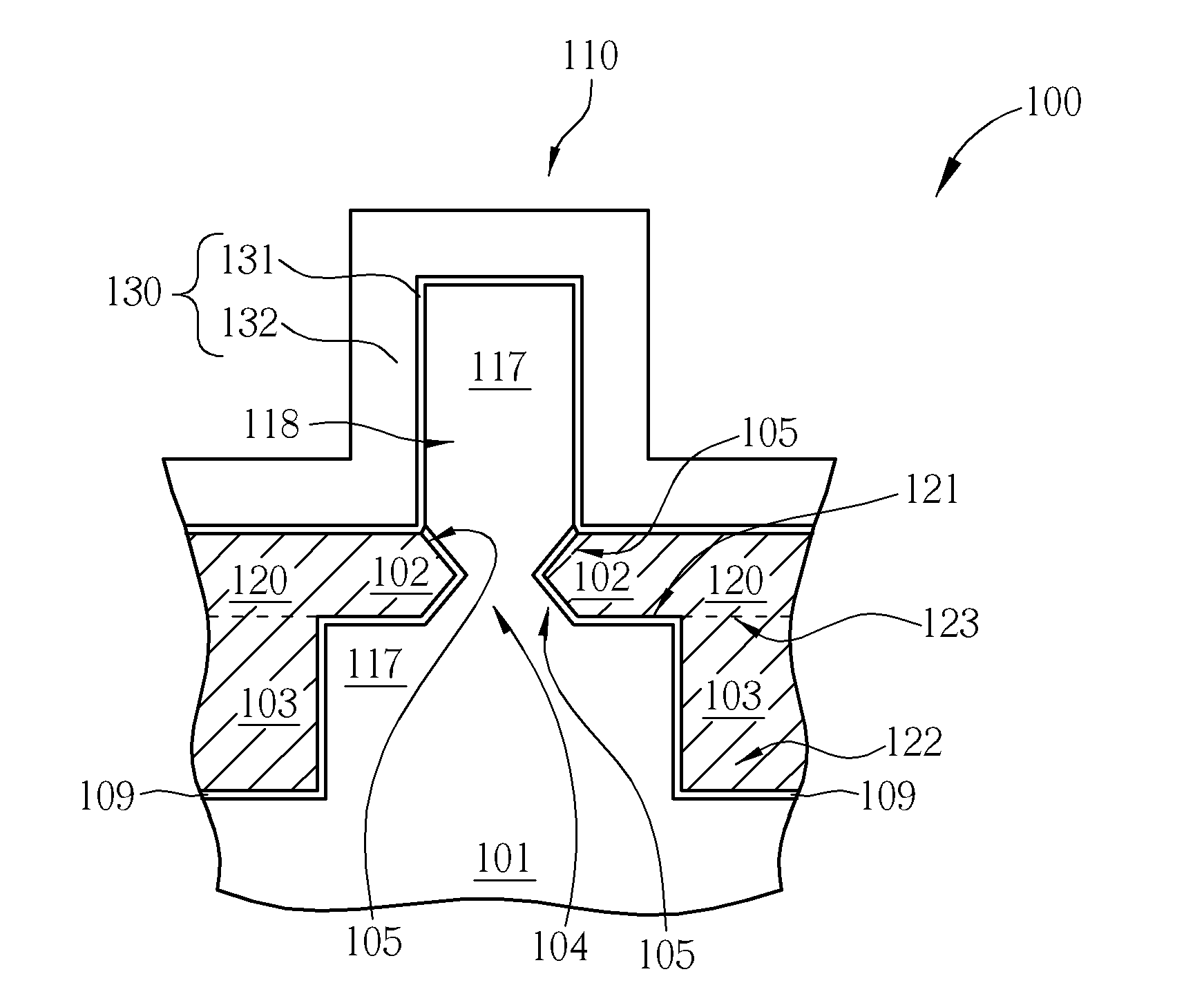
[0029]In the present invention, an oxide layer which fully supports the fin structure 110 is formed. Please refer to FIG. 6A, after the needed first recess 103 and second recess 102 are done, an oxidization procedure may be used to form the oxide layer 120 which fully supports the fin structure 110. For example, a furnace oxidation procedure is used to oxidize the exposed substrate 101, that is to oxidize the Si atoms in the substrate 101 near the fin structure 110, the first recess 103 and the second recess 102, to form a bulk oxide 120 including silicon oxide and serve as a field oxide to segregate the substrate 101 and the fin structure 110. The thickness of the bulk oxide layer 120 may be 10 nm˜200 nm and the bottle neck 104 vanishes because of the destructive oxidation procedure.

[0030]Owing to the introduction of oxygen atoms, the oxide layer 120 fills up the second recess 102 and occupies most of the first recess 103 so the first recess 103 barely remains. In addition, due to ...

second embodiment

[0032]In the present invention, an oxide layer which fully covers the fin structure 110 is formed. Please refer to FIG. 6B, after the needed first recess 103 and second recess 102 are done, a deposition procedure may be used to form the oxide layer 120 which fully covers the fin structure 110 and fully fills up the first recess 103 and second recess 102 without oxidizing the Si atoms in the substrate 101.

[0033]For example, a spin-on dielectric (SOD) which coats a layer of liquid containing silicon oxide on the wafer surface and / or a deposition procedure is used to form the oxide layer 120 which fully covers the fin structure 110, the first recess 103 and second recess 102 so that the insulating layer 120 may include silicon oxide or silicon oxynitride. SOD fills the gap to exhibit good coverage. A thermo annealing is carried out on the liquid to transform it to a solid oxide layer. Please note that the fin structure 110 is still directly connected to the substrate 101 because no Si ...


PUM


Abstract

A FINFET transistor structure includes a substrate, a fin structure, an insulating layer and a gate structure. The fin structure is disposed on the substrate and directly connected to the substrate. Besides, the fin structure includes a fin conductive layer and a bottle neck. The insulating layer covers the substrate and has a protruding side which is formed by partially surrounding the bottle neck of the fin structure, and a bottom side in direct contact with the substrate so that the protruding side extend to and under the fin structure. The gate structure partially surrounds the fin structure.

Description

BACKGROUND OF THE INVENTION[0001]1. Field of the Invention[0002]The present invention generally relates to a FINFET transistor structure and a method for forming various FINFET transistor structures. In particular, the present invention is directed to a method for forming various FINFET transistor structures by different possibilities of formation of oxide layers to reduce the leak current of the FINFET transistor structure or to maintain the heat-dissipating of the FINFET transistor structure.[0003]2. Description of the Prior Art[0004]One of the purposes of the development of the semiconductor industry is to enhance the efficiency of the semiconductor devices and to reduce the energy consumption of the semiconductor devices. When it comes to enhancing the efficiency of the semiconductor devices, it is already known in the prior art that different lattice structures may facilitate the mobility of the electrons or the holes.[0005]For example, a higher carrier mobility can be observed...

Claims


Application Information

Patent Timeline
IPC IPC(8): H01L29/786H01L21/3205
CPCH01L29/66795H01L29/785H01L29/0653H01L27/10826H01L29/7854H01L27/10879H10B12/36H10B12/056
Inventor HUANG, RAI-MINDAI, SHENG-HUEITSAI, CHEN-HUALIAO, DUAN QUANCHEN, YIKUNZHU, XIAO ZHONG
Owner UNITED MICROELECTRONICS CORP
Why Eureka
Try Eureka