Non-volatile memory device having a resistance-changeable element and method of forming the same

Active Publication Date: 2012-12-06
SAMSUNG ELECTRONICS CO LTD
View PDF4 Cites 8 Cited by
  • Summary
  • Abstract
  • Description
  • Claims
  • Application Information

AI Technical Summary

Benefits of technology

[0004]Example embodiments of the inventive concept provide a non-volatile memory device capable of preventing degradation in characteristics of a resistance-changeable element.
[0005]Example embodiments of the inventive concept also provide a method of forming a non-volatile memory device capable of preventing degradation in characteristics of a resistance-changeable element.

Problems solved by technology

This high temperature treatment and subsequent etching causes degradation of the desirable electrical performance characteristics of the TMO layer.

Method used


Image

  • Non-volatile memory device having a resistance-changeable element and method of forming the same
  • Non-volatile memory device having a resistance-changeable element and method of forming the same
  • Non-volatile memory device having a resistance-changeable element and method of forming the same

Examples


Embodiment Construction

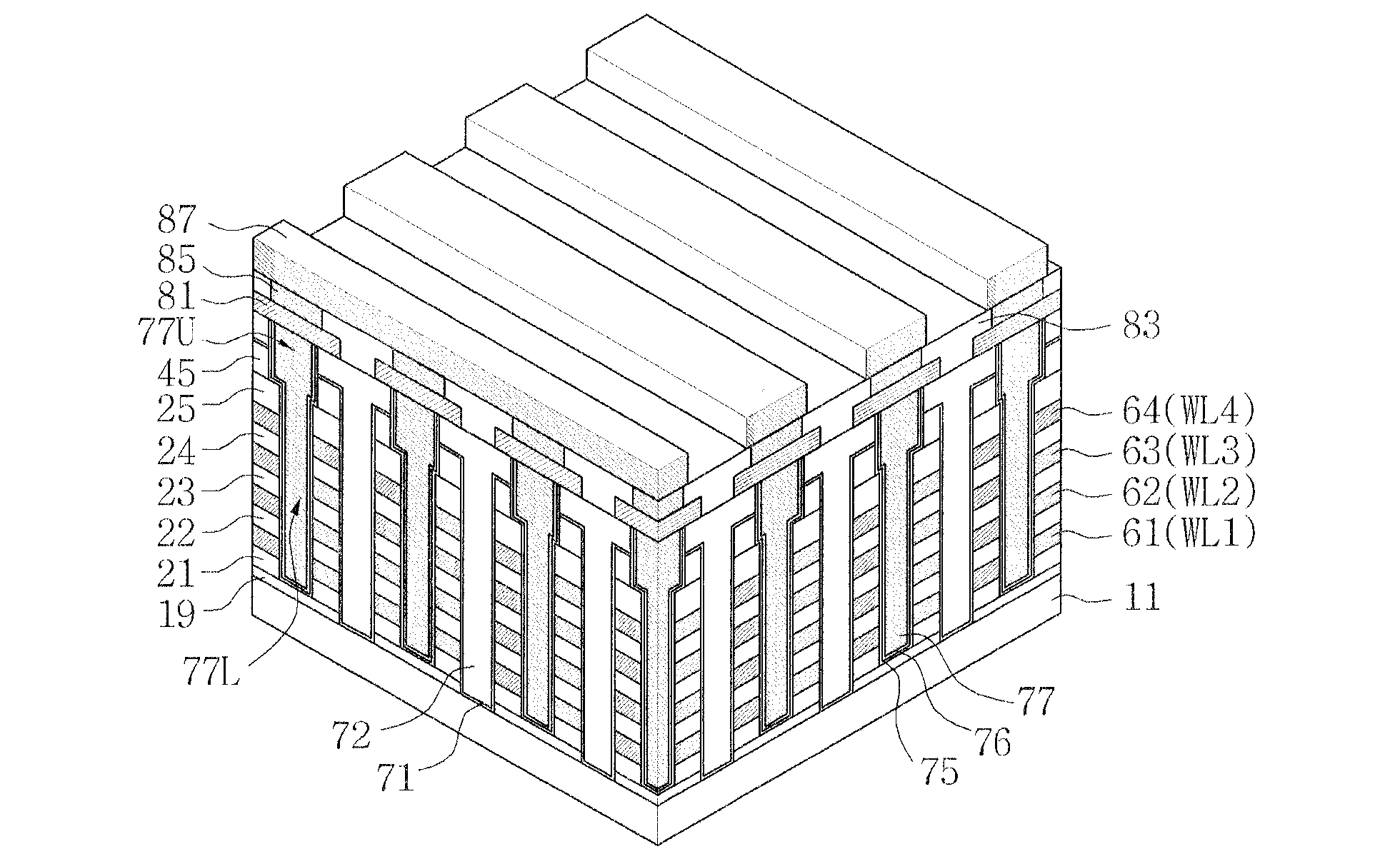
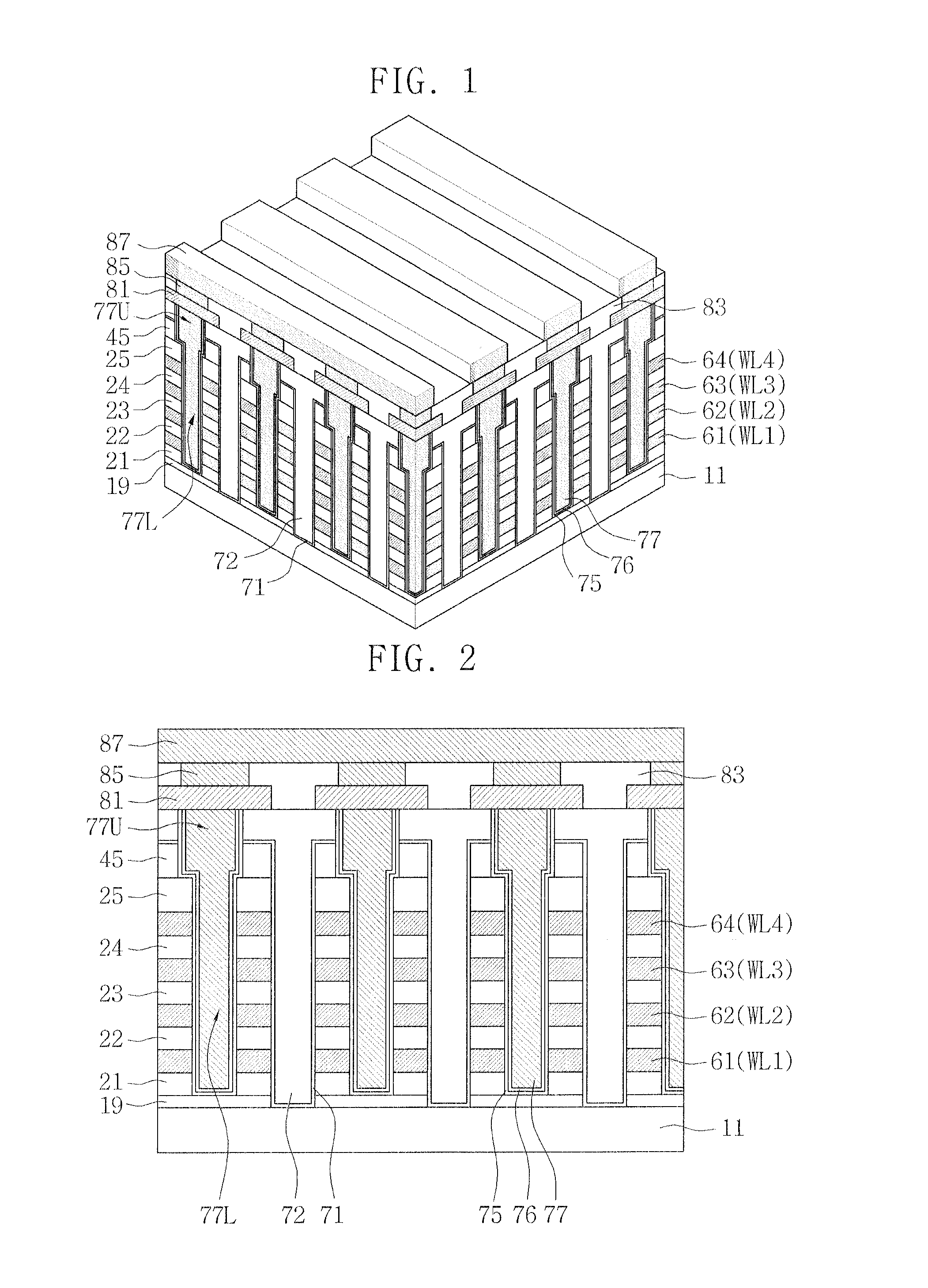
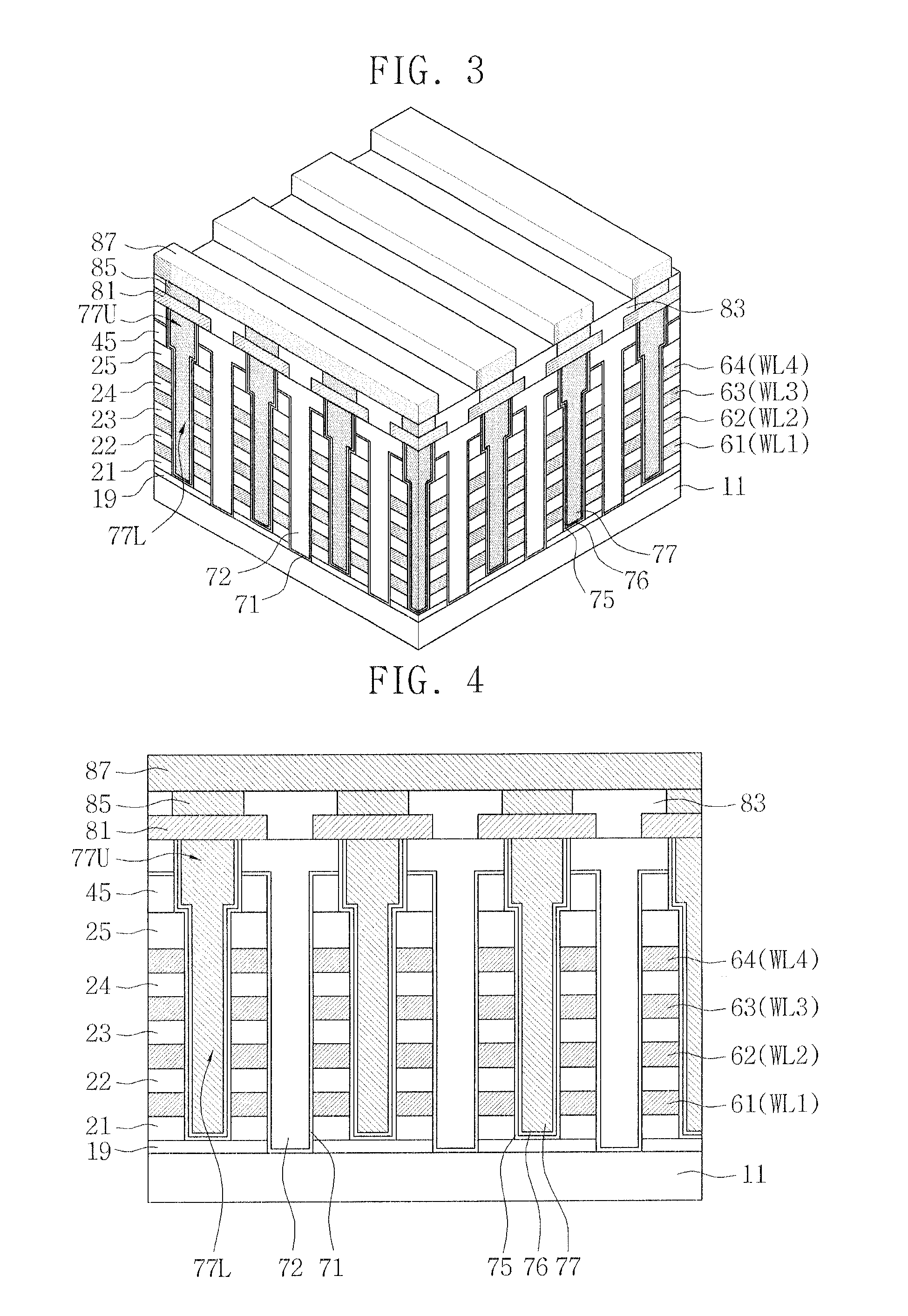
[0029]Detailed illustrative embodiments are disclosed herein. However, specific structural and functional details disclosed herein are merely representative for purposes of describing example embodiments. This inventive concept, however, may be embodied in many alternate forms and should not be construed as limited to only example embodiments set forth herein. In the drawings, like numbers refer to like elements throughout the description of the figures, and the thicknesses of layers and regions may be exaggerated for clarity. In addition, when it is described that a first element is disposed “on” or “above” a second element, it means that the first element may be disposed on and in directly contact with the second element, or a third element may be disposed between the first and second elements.

[0030]Here, it will be understood that, although the terms first, second, etc. may be used herein to describe various elements, these elements should not be limited by these terms. These ter...


PUM


Abstract

A non-volatile memory device is provided wherein a lower molding layer is formed on a substrate; a first horizontal interconnection is formed on the lower molding layer; an upper molding layer is formed on the first horizontal interconnection; a pillar is formed connected to the substrate by vertically passing through the upper molding layer, the first horizontal interconnection and the lower molding layer. The pillar has a lower part and an upper part, wherein the lower part is disposed on the same level as the first horizontal interconnection and has a first width and the upper part is disposed on a higher level than the first horizontal interconnection and has a second width different from the first width.

Description

CROSS-REFERENCE TO RELATED APPLICATION[0001]This application claims priority under 35 U.S.C. §119 to Korean Patent Application No. 10-2011-0054072 filed on Jun. 3, 2011, the disclosure of which is hereby incorporated by reference in its entirety.TECHNICAL FIELD [0002]Example embodiments of the inventive concept relate to a non-volatile memory device having a plurality of memory cells which are vertically stacked, and a method of forming the same.DESCRIPTION OF THE RELATED ART [0003]A transition-metal-oxide (TMO) layer is a major component of a Resistive Random Access Memory chip (RRAM), and is sensitive to heat during manufacturing. In a conventional vertical structure manufacturing processes, after the formation of the TMO layer, the layer is exposed to a high temperature which may be as high as 500° C. or more. This high temperature treatment and subsequent etching causes degradation of the desirable electrical performance characteristics of the TMO layer. In order to obtain a non...

Claims


Application Information

Patent Timeline
IPC IPC(8): H01L47/00
CPCH01L45/04H01L27/249H01L45/146H01L45/1226H10B63/845H10N70/20H10N70/823H10N70/8833H10B63/20
Inventor JU, HYUN-SUKIM, SUN-JUNGCHAE, SOO-DOO
Owner SAMSUNG ELECTRONICS CO LTD
Why Eureka
Try Eureka