
Semiconductor device and method of manufacturing the same

a semiconductor and semiconductor technology, applied in the direction of semiconductor devices, electrical appliances, transistors, etc., can solve the problems of lowering the threshold voltage (vt) of the transistor, deterioration of refresh characteristics, and increase of junction leakage current, so as to reduce channel resistance and facilitate and favorably manufacture

Inactive Publication Date: 2012-12-06
PS4 LUXCO SARL
View PDF5 Cites 10 Cited by
  • Summary
  • Abstract
  • Description
  • Claims
  • Application Information

AI Technical Summary

Benefits of technology

The semiconductor device described in this patent has several technical effects. Firstly, it has two channel regions, which reduces channel resistance and maintains the ON current of the transistor. Secondly, it has a structure where no channel region is formed between the gate grooves, which allows for independent operation of transistors. Lastly, the semiconductor device has a structure where the gate electrode does not protrude upward from the surface of the semiconductor substrate, which makes it easier to manufacture a DRAM.

Problems solved by technology

The technical problem addressed in this patent text is the difficulty in miniaturizing transistors in a semiconductor device such as a dynamic random access memory (DRAM) without compromising the threshold voltage of the transistor and ensuring stable operation of each transistor independently. Additionally, the challenge of forming bit wiring and capacitors in the DRAM manufacturing process arises from the use of a trench gate transistor. The invention aims to provide a semiconductor device with a sufficient ON current of a transistor without interference between adjacent transistors and a method of manufacturing the semiconductor device without difficulties in the manufacture process.

Method used


Image

  • Semiconductor device and method of manufacturing the same
  • Semiconductor device and method of manufacturing the same
  • Semiconductor device and method of manufacturing the same

Examples


first embodiment

(Semiconductor Device)

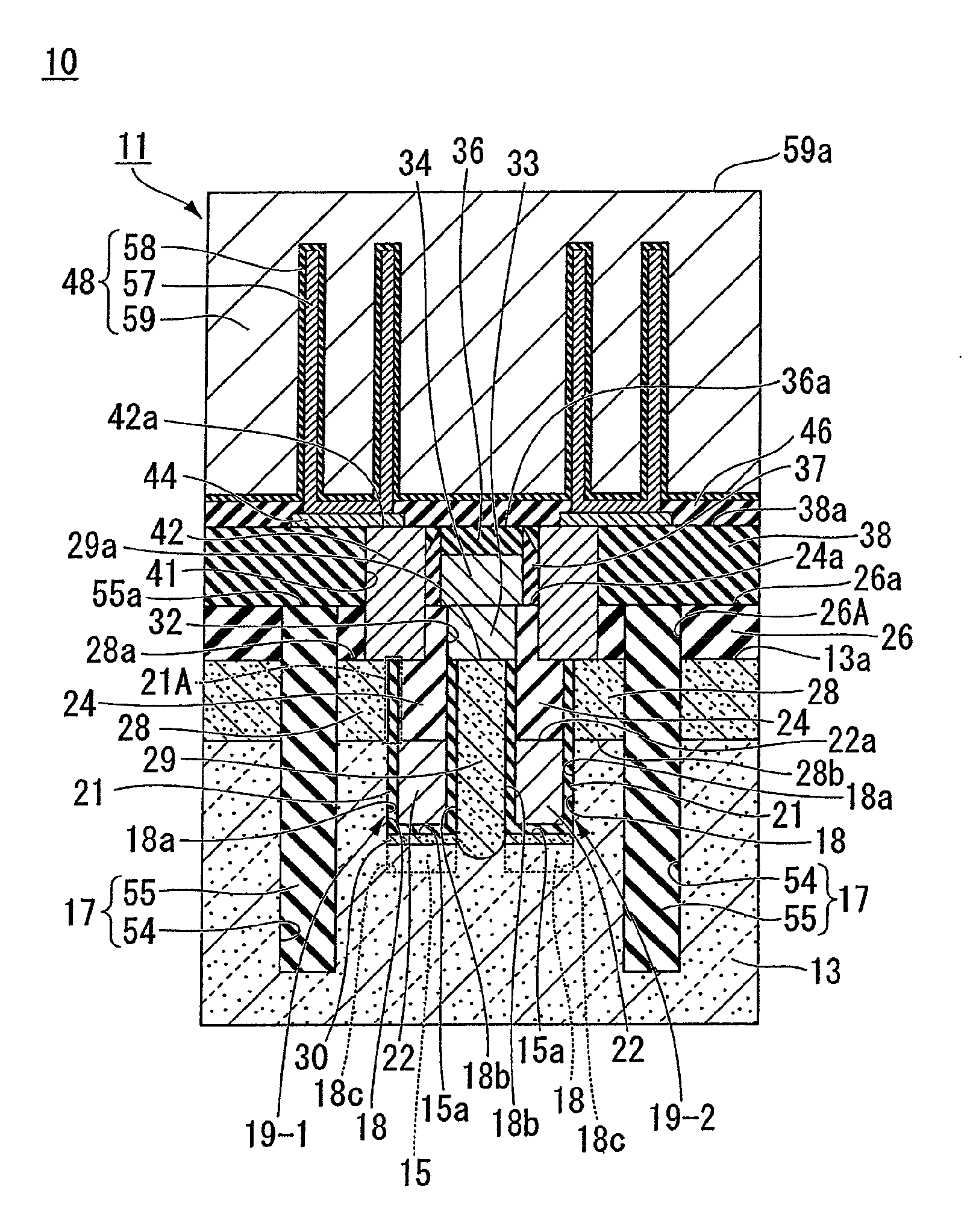
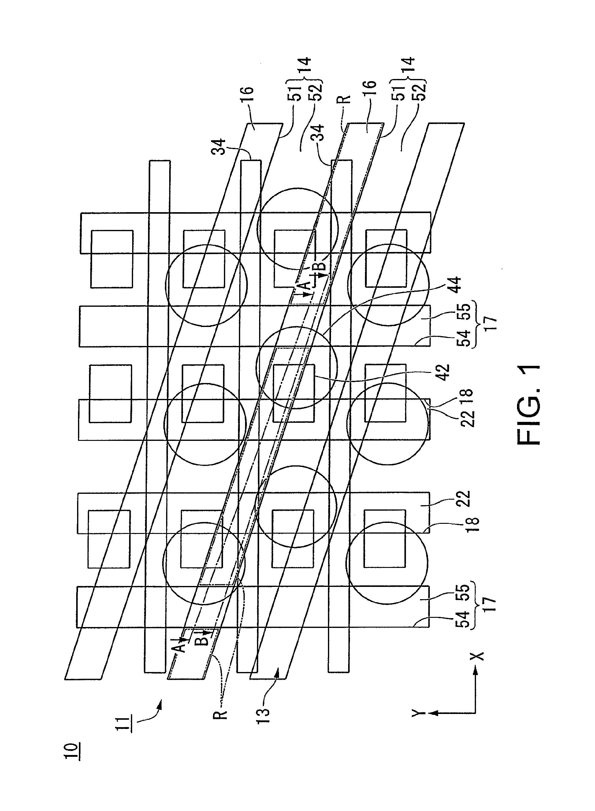
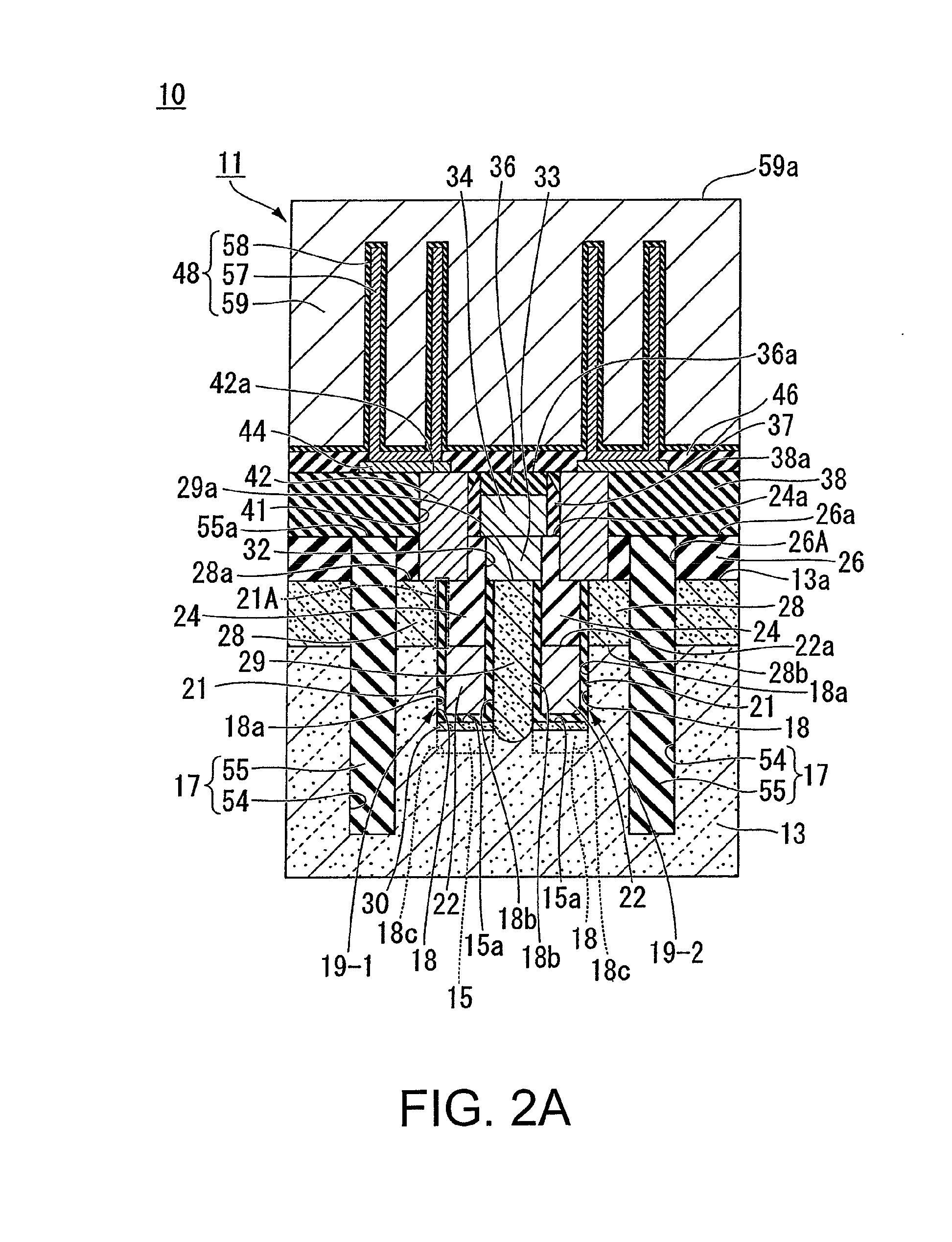
[0112]FIG. 1 is a schematic plan view of a memory cell array provided in a semiconductor device according to a first embodiment of this invention. FIG. 2A is a sectional view taken along the line A-A of the memory cell array illustrated in FIG. 1. FIG. 2B is a sectional view of the memory cell array taken along the line B-B of FIG. 1. FIG. 2C is a perspective view illustrating a structure in section of a fin portion provided in a gate groove in the semiconductor device according to the first embodiment. FIG. 2D is an enlarged view around the gate groove and the fin portion and is a sectional view illustrating an internal structure around the fin portion.

[0113]In FIG. 1, FIG. 2A, and FIG. 2B, a dynamic random access memory (DRAM) is illustrated as an example of a semiconductor device 10 as the first embodiment according to this invention. Further, FIG. 1 illustrates an exemplary layout of a memory cell array of the DRAM.

[0114]In FIG. 1, bit lines 34 extend along...

second embodiment

[0311]Next, a memory cell array provided in a semiconductor device according to a second embodiment of this invention and a method of manufacturing the memory cell array are described in detail with reference to FIG. 19A and FIG. 19B.

[0312]As illustrated in FIG. 19A and FIG. 19B, a structure of a semiconductor device 210 according to the second embodiment is different from the above-mentioned structure of the semiconductor device 10 according to the first embodiment in that the semiconductor device 210 illustrated in FIGS. 19A and 19B includes, as a first carrier capture region 230, the carrier capture region 30 mentioned in conjunction with the first embodiment and a second carrier capture region 31. Other points of the structure are the same as those of the first embodiment. Therefore, with regard to the structure of the semiconductor device and the method of manufacturing the same according to this embodiment, like reference symbols are used to designate like or identical members...


PUM


Abstract

Provided are a semiconductor device capable of increasing an ON current with a reduced channel resistance, and also capable of stably and independently operating respective transistors, and a method of manufacturing the semiconductor device. A semiconductor device includes a fin portion located in a manner that a part of an active region protrudes from a bottom portion of a gate groove, a gate insulating film for covering the gate groove and a surface of the fin portion, a gate electrode which is embedded within a lower portion of the gate groove and formed so as to straddle the fin portion via the gate insulating film, a first diffusion region, a second diffusion region, and a carrier capture region provided in the surface of the fin portion.

Description


Claims


Application Information

Patent Timeline
Owner PS4 LUXCO SARL
Learn More