

Semiconductor process and structure thereof
a technology of semiconductors and oxide layers, applied in the direction of semiconductor devices, electrical equipment, basic electric elements, etc., can solve the problems of inferior performance, reduced gate capacitance, and conventional polysilicon gate, and achieve the effect of enhancing the density of the oxide layer and improving the performance of the semiconductor structur
- Summary
- Abstract
- Description
- Claims
- Application Information
AI Technical Summary
Benefits of technology
Problems solved by technology
Method used
Image

Examples
Embodiment Construction
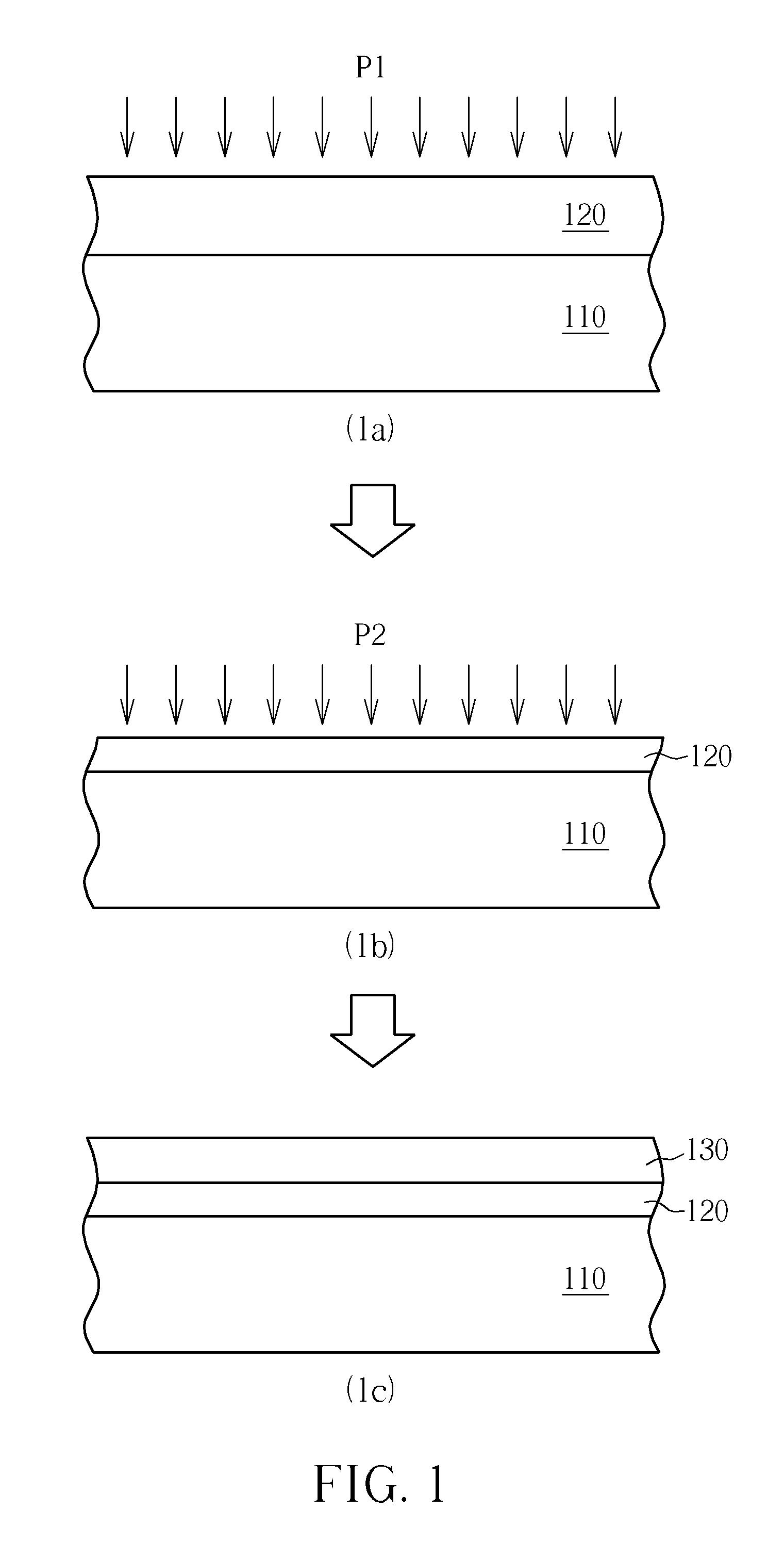
[0023]FIG. 1 schematically depicts a cross-sectional view of a semiconductor process according to one embodiment of the present invention. As shown in FIG. 1a, a substrate 110 is provided. An oxidation process P1 is performed on the substrate 110 to form an oxide layer 120 on the surface of the substrate 110. The substrate 110 may be a semiconductor substrate such as a silicon substrate, a silicon-containing substrate or a silicon-on-insulator (SOI) substrate. In this embodiment, the substrate 110 is a silicon substrate, so that the oxide layer 120 is a silicon dioxide layer formed by performing the oxidation process P1 to oxidize the silicon substrate, but it is not limited thereto. Otherwise, the oxidation process P1 may be a wet oxidation process such as an in situ steam generation (ISSG) oxidation process, a dry oxidation process etc. When the process temperature of the oxidation process P1 is high or the process time of the oxidation process P1 is long, an oxide layer 120 havin...
PUM
 Abstract
Description
Claims
Application Information