Liquid crystal device, projection type display device, and electronic apparatus

Inactive Publication Date: 2012-12-06
SEIKO EPSON CORP
View PDF1 Cites 18 Cited by
  • Summary
  • Abstract
  • Description
  • Claims
  • Application Information

AI Technical Summary

Benefits of technology

[0108]As described above, according to the liquid crystal device 100 of the embodiment, the data line driving circuit 101 (first driving circuit unit) inverts the polarities of the pixel electrodes 9a on the element substrate 10 side and the common electrode 21 on the opposing substrate 20 side during the first period T1 and the second period T2. Further, the trapping electrode driving circuit unit 80 (second driving circuit unit) drives the first electrode 81 and the second electrode 82 on the element substrate 10 side corresponding to such inversion driving. Here, the polarity of the first electrode 81 with respect to the third electrode 83 on the opposing substrate 20 side is the opposite to the polarity of the pixel electrodes 9a with respect to the common electrode 21, and the polarity of the second electrode 82 with respect to the third electrode 83 on the opposing substrate 20 side is the same as the polarity of the pixel electrodes 9a with respect to the common electrode 21. That is, the polarity between the element substrate 10 and the opposing substrate 20 inverts for every region from the image display region 10a toward the outside. Therefore, if the first period T1 and the second period T2 are repeated, the ionic impurities within the image display region 10a are sequentially trapped in each region by the polarity between the element substrate 10 and the opposing substrate 20 and efficiently ejected from the inside to the outside of the image display region 10a by the flow of the liquid crystal layer 50 which is generated due to the oscillation of the liquid crystal molecules 50b.
[0109]Further, in the first period T1, while an image signal with the potential Vs(+) that is higher than the common potential Vcom is applied to the pixel electrodes 9a, since the potential Vs(−) that is lower than the common potential Vcom is applied to the first electrode 81, the potential difference between the first electrode 81 and the pixel electrodes 9a is large. The ionic impurities that are within the image display region 10a are therefore efficiently ejected from the inside to the outside of the image display region 10a. Further, similarly to the first period T1, the ionic impurities within the image display region 10a are also efficiently ejected from the inside to the outside of the image display region 10a during the second period T2.
[0110]Moreover, according to the embodiment, the trapping electrode driving circuit unit 80 supplies the potential Vf(−) that is lower than the common potential Vcom to the first electrode 81 and supplies the potential Vf(+) that is higher than

Problems solved by technology

With such a liquid crystal device, if ionic impurities that are mixed in when the liquid crystal is injected or ionic impurities that are eluted from the sealing material agglomerate within the image display region as the liquid crystal device is driven, deterioration in the display quality, such as burn-in (staining) of the image, occur.
However, with a configuration of drawing in ionic impurities to the first and second electrodes by a direct current voltage that is applied between the first electrode on the element substrate side and the second electrode on the opposing substrate side as with the configuration described in FIG. 1 of JP-A-2002-196355, the capability of drawing in and retaining the ionic impurities is low.
Further, in a case when a driving method of inverting the

Method used


Image

  • Liquid crystal device, projection type display device, and electronic apparatus
  • Liquid crystal device, projection type display device, and electronic apparatus
  • Liquid crystal device, projection type display device, and electronic apparatus

Examples


embodiment 1

[0037]In Embodiment 1 of the invention, first, a case when a first electrode and a second electrode are provided on the element substrate side will be described.

Electrical Configuration of Image Display Region and the Like

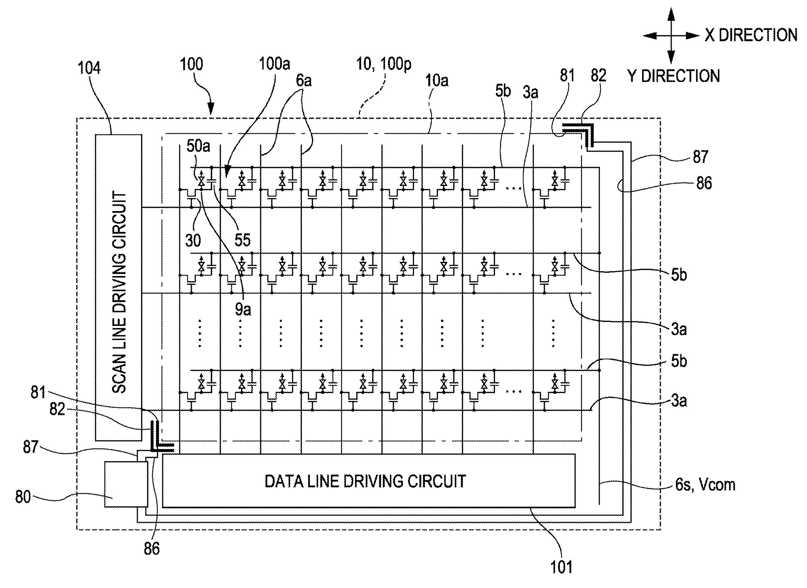
[0038]FIG. 1 is a block diagram that illustrates an electrical configuration of a liquid crystal device according to Embodiment 1 of the invention. Here, FIG. 1 is merely a block diagram that illustrates an electrical configuration, and does not illustrate wiring, the shape or the extending directions of the electrodes, the layout, or the like.

[0039]In FIG. 1, a liquid crystal device 100 includes a liquid crystal panel 100p of a TN (Twisted Nematic) mode or a VA (Vertical Alignment) mode, and the liquid crystal panel 100p includes an image display region 10a (pixel arrangement region, effective pixel region) in which a plurality of pixels 100a are arranged in a matrix form in the central region thereof. With the liquid crystal panel 100p, a plurality of data lines ...

second embodiment

[0114]FIG. 8 is an explanatory diagram of the electrodes and the like that are formed on a liquid crystal device 100 according to Embodiment 2 of the invention. Here, since the basic configuration of the embodiment is the same as Embodiment 1, the same symbols are given to common portions, and description thereof will be omitted.

[0115]While the third electrode 83 was configured as a portion of the common electrode 21 on the opposing substrate 20 in Embodiment 1, in the present embodiment, the third electrode 83 is configured as a separate electrode that is separated from the common electrode 21 as illustrated in FIG. 8. According to such a configuration, if the same potential is set for the third electrode 83 and the common electrode 21, the potential described with reference to FIGS. 6A to 6C may be supplied to each electrode. That is, the polarities on the element substrate 10 side and the opposing substrate 20 side during the first period T1 and the second period T2 are as below....

third embodiment

[0172]FIG. 9 is an explanatory diagram of the electrodes and the like that are formed on the element substrate 10 of a liquid crystal device 100 according to Embodiment 3 of the invention. Here, FIG. 9 is illustrated with a reduced number and the like of the pixel electrodes 9a. Further, since the basic configuration of the embodiment is the same as Embodiment 1, the same symbols are given to common portions, and description thereof will be omitted.

[0173]While one each of the first electrode 81 and the second electrode 82 were provided in the corners 10a1 and 10a3 in Embodiment 1, as illustrated in FIG. 9, a configuration in which each of the first electrode 81 and the second electrode 82 are alternately provided in a plurality from the image display region 10a toward the sealing material 107 may be adopted. Here, in FIG. 9, although a configuration in which two each of the first electrode 81 and the second electrode 82 are provided alternately from the image display region 10a towa...


PUM


Abstract

The polarities of pixel electrodes and a common electrode are inverted and a first electrode and a second electrode on an element substrate side are driven during a first period and a second period. At this time, the polarity of the first electrode with respect to a third electrode on an opposing substrate side is the opposite to the polarity of the pixel electrodes with respect to the common electrode, and the polarity of the second electrode with respect to the third electrode on the opposing substrate side is the same as the polarity of the pixel electrodes with respect to the common electrode.

Description

BACKGROUND[0001]1. Technical Field[0002]The present invention relates to a liquid crystal device in which a liquid crystal layer is retained between a pair of substrates, a projection type display device that uses the liquid crystal device as a light valve, and an electronic apparatus.[0003]2. Related Art[0004]With a liquid crystal device, an element substrate on which an image display region in which a plurality of pixel electrodes are arranged on one face side is provided and an opposing substrate on which a common electrode is provided to which a common potential is applied are pasted together by a sealing material, and a liquid crystal layer is held within a region that is surrounded by the sealing material between the element substrate and the opposing substrate. With such a liquid crystal device, if ionic impurities that are mixed in when the liquid crystal is injected or ionic impurities that are eluted from the sealing material agglomerate within the image display region as ...

Claims


Application Information

Patent Timeline
IPC IPC(8): G02F1/1335G02F1/1343
CPCG02F1/1343G02F2001/133388G09G3/3614G09G2320/046G09G2300/0426G09G2310/0232G09G3/3648G02F1/133388
Inventor TANAKA, TAKAAKI
Owner SEIKO EPSON CORP
Why Eureka
Try Eureka