Package carrier and package structure

a technology of packaging and packaging, applied in the direction of semiconductor devices for light sources, semiconductor/solid-state device details, lighting and heating apparatus, etc., can solve the problems of led chip decay, permanent damage, and low heat dissipation effect, and achieve the effect of improving heat dissipation

Inactive Publication Date: 2012-12-13
SUBTRON TECH
View PDF7 Cites 17 Cited by
  • Summary
  • Abstract
  • Description
  • Claims
  • Application Information

AI Technical Summary

Benefits of technology

[0025]Based on the depiction above, the design of the package carrier in the invention features that the dielectric layer extends from the main mounting surface of the carrier up, along boundaries between the main mounting surface and the side mounting surfaces, onto the side mounting surfaces by using the flexibility property thereof, and the heat-generating elements are located on a portion of the main mounting surface and portions of the side mounting surfaces of the carrier exposed by the first openings of the dielectric layer. In this way, when the heat-generating elements are, for example, a plurality of LED chips, the package structure of the invention can have light-emitting effect with three-dimensional polyhedron. In addition, the heat of the heat-generating elements can be directly and fast transmitted outwards through the carrier, so that the package structure of the invention has better heat-dissipating effect.

Problems solved by technology

If the thermal energy produced by the LED chip is not dissipated and accumulated in the LED package structure, the temperature of the LED package structure may steadily rise.
As a result, the LED chip has a decayed luminance and a shorter lifetime due to the above-mentioned over heat, and even more seriously, gets permanent damage.
However, since the heat-conducting rate of the adhesive layer and the insulation layer is poor, during the heat produced by the LED chip is being transmitted to the heat sink via the patterned conductive layers and the insulation layer, the thermal resistance established by the transmitting path would be increased, which results in heat-conducting difficulty.
It can be seen the quantities of the package substrates and the circuit substrates required by the above-mentioned LED package structure with light-emitting effect with three-dimensional polyhedron are quite many, which results in higher fabrication cost, more difficulty and more complexity of the process with the conventional LED package structure.

Method used


Image

  • Package carrier and package structure
  • Package carrier and package structure
  • Package carrier and package structure

Examples


Embodiment Construction

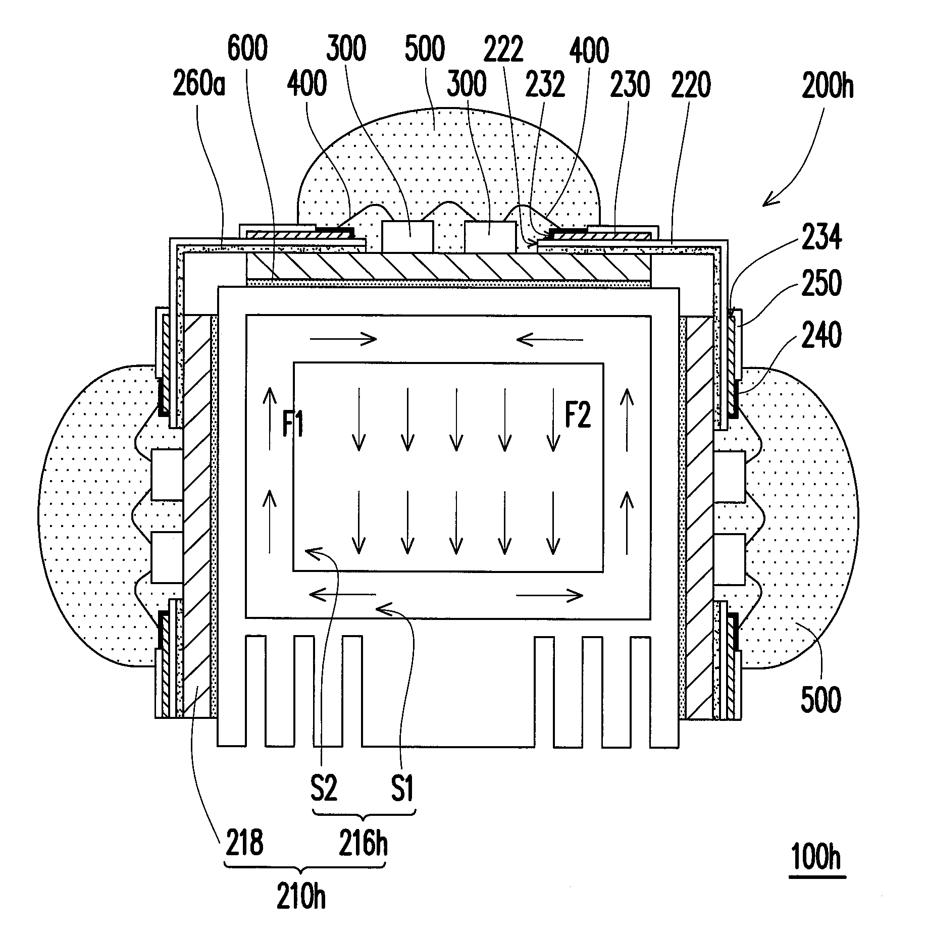
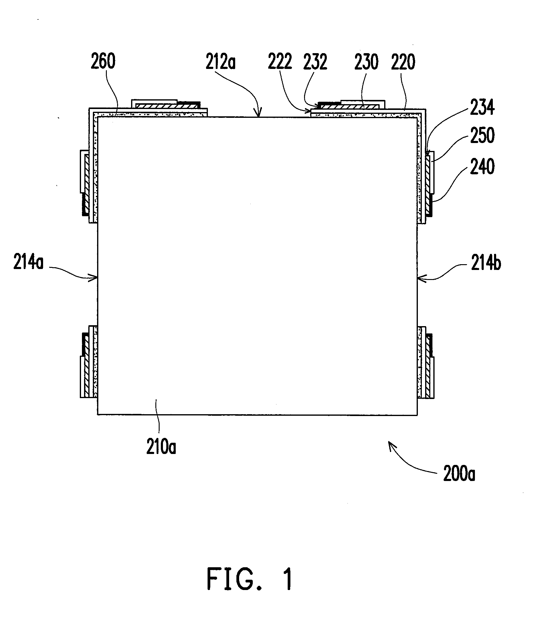
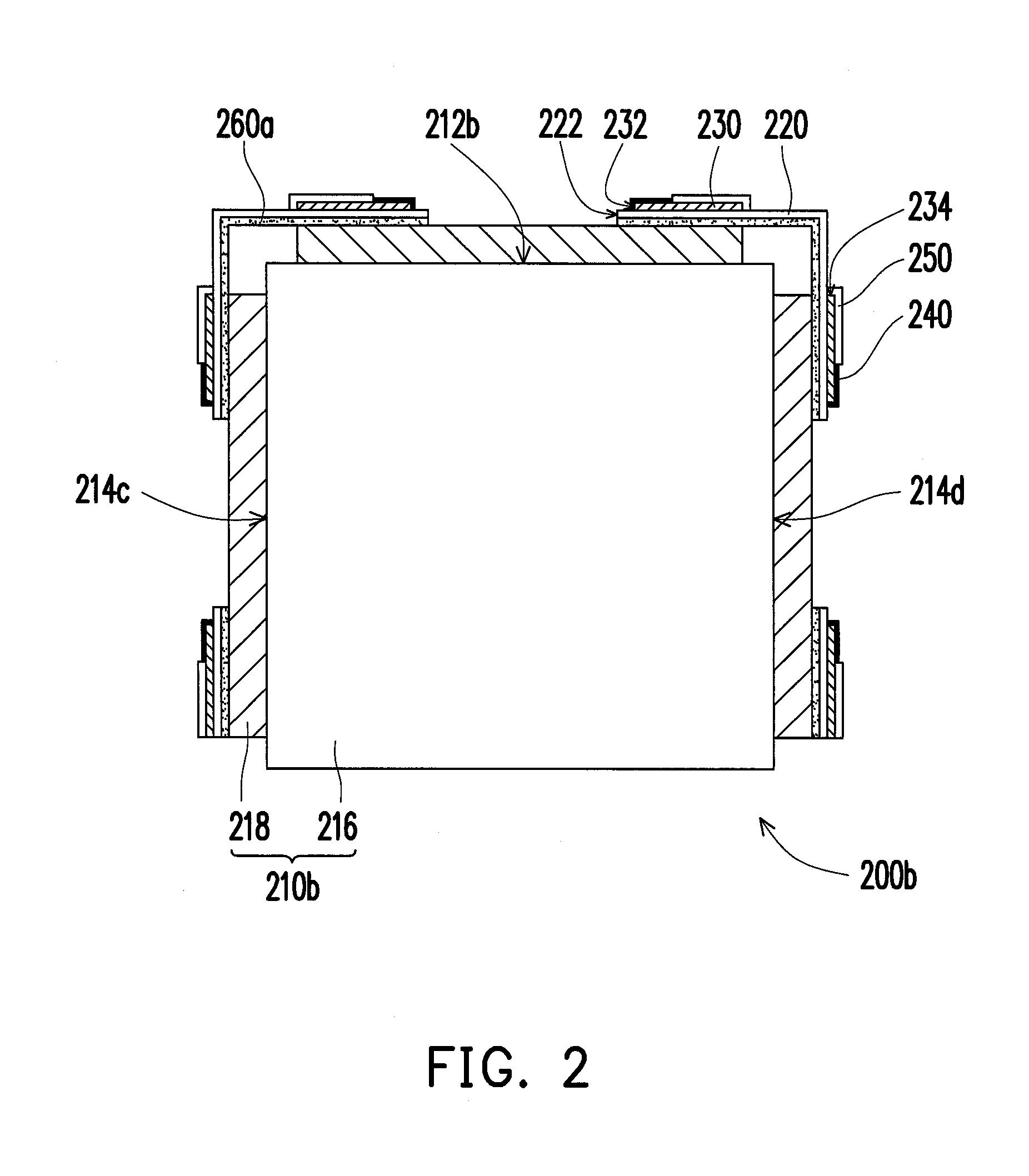
[0041]FIG. 1 is a cross-sectional diagram of a package carrier according to an embodiment of the invention. Referring to FIG. 1, in the embodiment, a package carrier 200a includes a carrier 210a, a dielectric layer 220, a metal layer 230, a surface treatment layer 240 and a solder resist layer 250. In more details, the carrier 210a has a main mounting surface 212a and at least two side mounting surfaces 214a and 214b connecting the main mounting surface 212a, in which the carrier 210a is, for example, a heat sink, a heat-dissipating fin, a thermal tube or a vapor chamber heat block. The carrier 210a herein is a heat sink as an example.

[0042]The dielectric layer 220 is disposed on the carrier 210a and has a plurality of first openings 222. In the embodiment, the package carrier 200a further includes an adhesive layer 260, and the dielectric layer 220 is adhered onto the carrier 210a through the adhesive layer 260, in which the dielectric layer 220 and the adhesive layer 260 are confo...


PUM


Abstract

A package carrier includes: a carrier having a main mounting surface and at least two side mounting surfaces connecting the main mounting surface; a dielectric layer disposed on the carrier, having multiple first openings and extending from the main mounting surface up, along boundaries between the main mounting surface and the side mounting surfaces, onto the side mounting surfaces, in which the first openings expose a portion of the main mounting surface and portions of the side mounting surfaces; a metal layer disposed on the dielectric layer and having multiple second openings disposed correspondingly to the first openings and multiple third openings exposing the partial dielectric layer at the above-mentioned boundaries; a surface treatment layer disposed on the partial metal layer; and a solder resist layer disposed on a portion of the metal layer and a portion of the dielectric layer both exposed out of the surface treatment layer.

Description

CROSS-REFERENCE TO RELATED APPLICATION[0001]This application claims the priority benefit of Taiwan application serial no. 100120569, filed on Jun. 13, 2011. The entirety of the above-mentioned patent application is hereby incorporated by reference herein and made a part of this specification.BACKGROUND OF THE INVENTION[0002]1. Field of the Invention[0003]The invention generally relates to a package carrier and a package structure, and more particularly, to a package carrier and a package structure with better heat-dissipating effect.[0004]2. Description of Related Art[0005]In terms of currently common light-emitting diode (LED) package structures, the LED chip thereof needs to be packaged prior to usage and a lot of thermal energy is produced by the LED chip during emitting light. If the thermal energy produced by the LED chip is not dissipated and accumulated in the LED package structure, the temperature of the LED package structure may steadily rise. As a result, the LED chip has ...

Claims


Application Information

Patent Timeline
Patent Type & Authority Applications(United States)
IPC IPC(8): H05K7/20H05K1/00
CPCH01L23/427H01L33/642H05K1/0206H05K1/021H05K1/05H05K3/0061F21V29/70H05K2201/10106F21Y2101/02F21Y2111/007H01L2224/48137H01L2224/48227H05K2201/047F21Y2115/10F21Y2107/40
Inventor WU, CHIEN-NAN
Owner SUBTRON TECH
Why Eureka
Try Eureka