Obsolescence tolerant flash memory architecture and physical building block (PBB) implementation

a flash memory and obsolescence-tolerant technology, applied in the direction of electrical apparatus construction details, electrical apparatus casings/cabinets/drawers, instruments, etc., can solve the problems of undesirable cost and labor time associated with re-certification, easy rework, and undesirable cost and labor for upgrades

Active Publication Date: 2012-12-20
BAE SYSTEMS CONTROLS INC
View PDF1 Cites 6 Cited by
  • Summary
  • Abstract
  • Description
  • Claims
  • Application Information

AI Technical Summary

Problems solved by technology

The cost and labor time associated with the re-certification are both undesirable.
Therefore, known electronic devices do not readily allow for rework such as upgrading, e.g., increasing memory in the electronic device, thus resulting in undesirable cost and labor for upgrades, as well as re-certifications.

Method used


Image

  • Obsolescence tolerant flash memory architecture and physical building block (PBB) implementation
  • Obsolescence tolerant flash memory architecture and physical building block (PBB) implementation
  • Obsolescence tolerant flash memory architecture and physical building block (PBB) implementation

Examples


Embodiment Construction

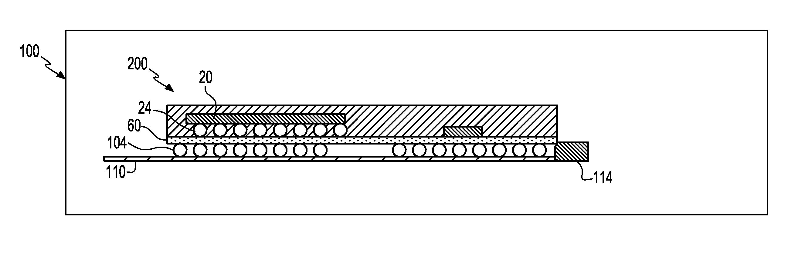
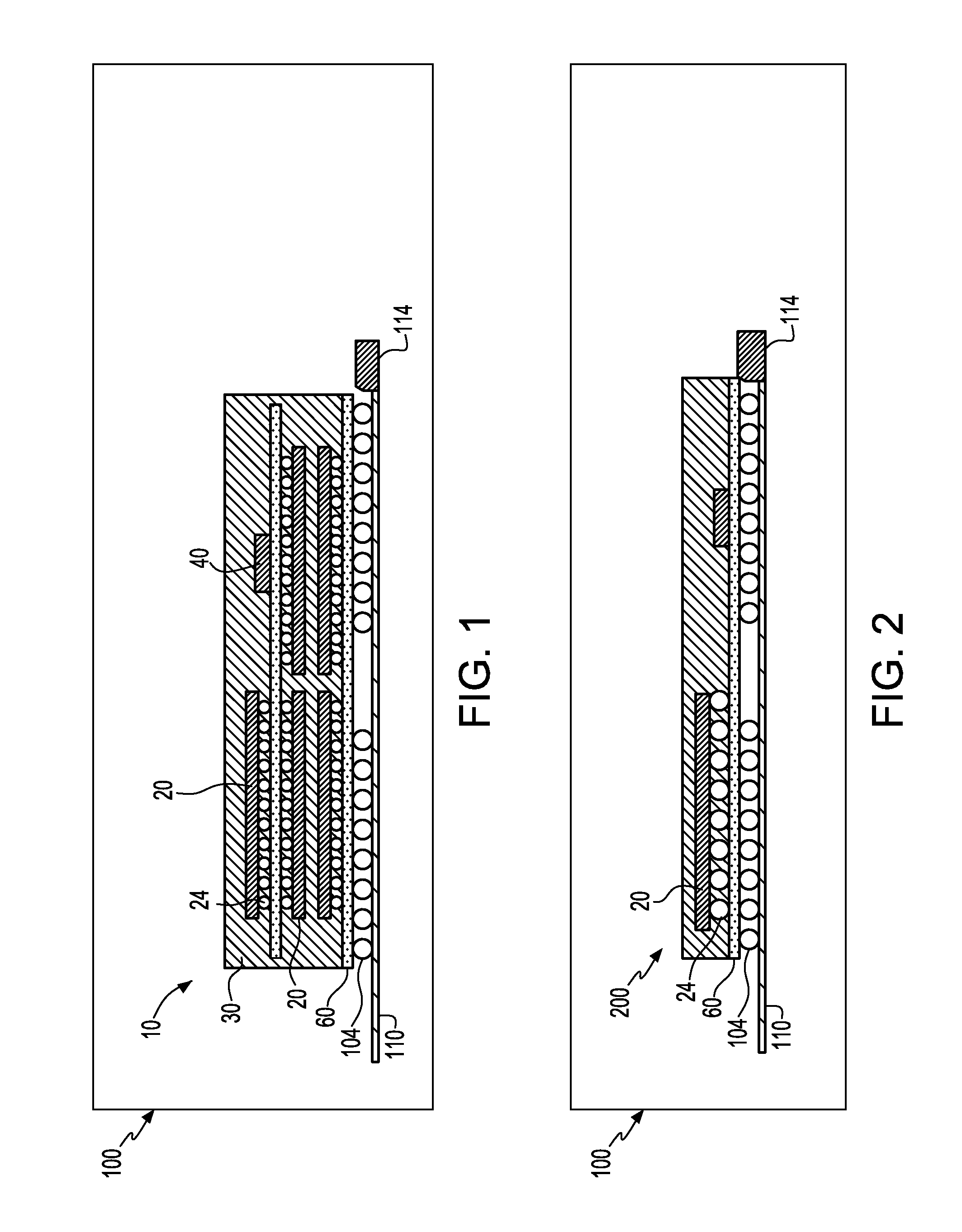
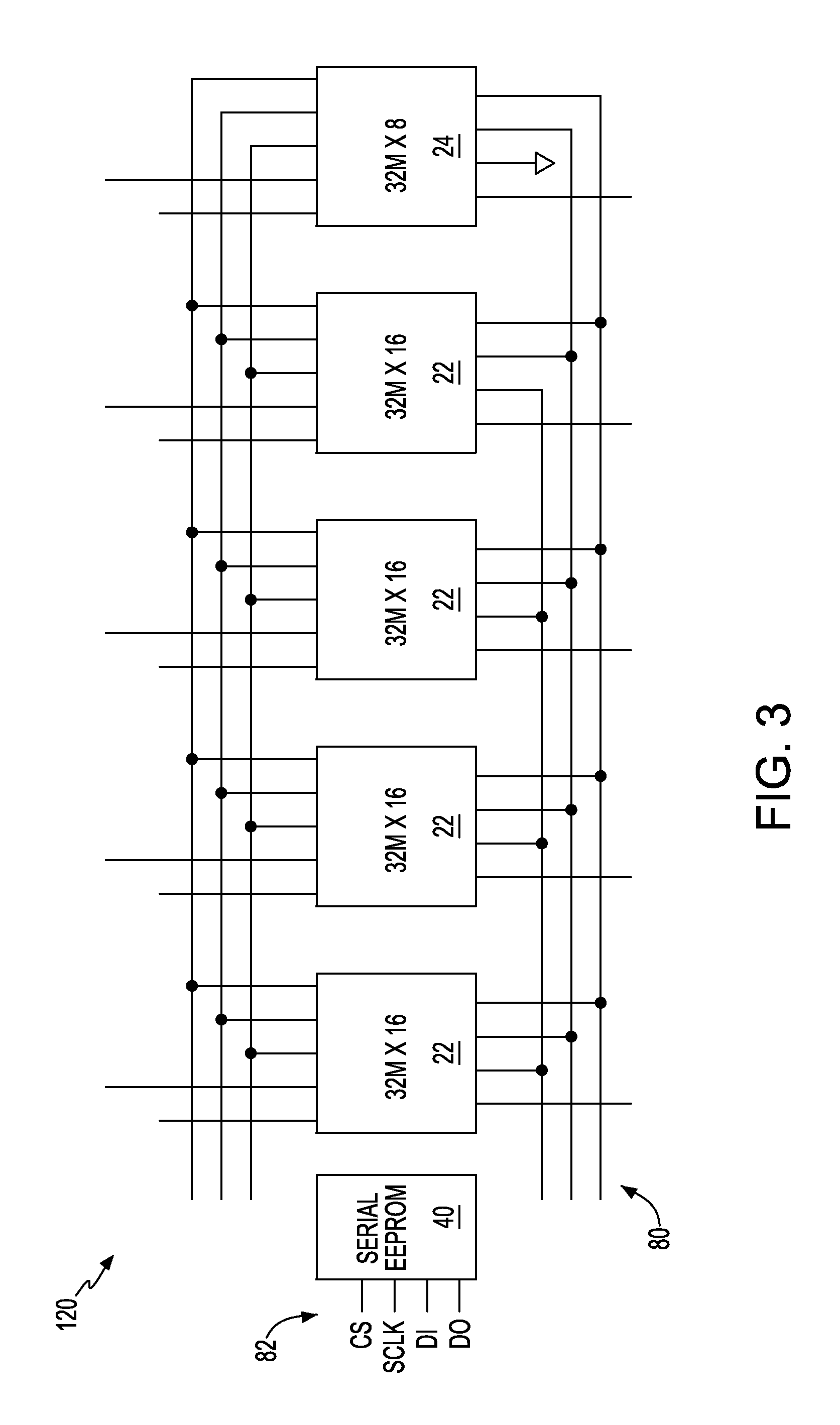
[0013]Referring to FIG. 1, an embodiment of the invention includes an electronic module embodied as a semiconductor module 10 for updating an electronic device 100. The electronic module or semiconductor module 10 may be a physical building block (PBB) module. A PBB may use a combination of advanced system in package (SIP) technologies. The SIP technologies may include, for example: a bare die such as wire bond or flip chip technologies; a stacked die; wafer level packages; an assembled die; and stacked packages. The electronic module 10 is a stacked die type of module or package, or may be considered an encapsulated package.

[0014]The electronic module 10 is connected to a circuit board 110 having, for example, a memory interface embodied as a processor, wherein the processor is embodied as a central processing unit (CPU) 114 for the electronic device 100. In the embodiment of the invention shown in FIG. 4, a processor is embodied as a CPU 114, however, any memory interface may be u...


PUM

PropertyMeasurementUnit
electrical schematic diagramaaaaaaaaaa
surface areaaaaaaaaaaa

Abstract

An electronic module and method for updating an electronic device wherein the electronic module is connected to a circuit board having one or more memory interfaces which may be embodied as processors in the electronic device. One or more semiconductor devices electrically communicate with an electrical circuit within the module. A programmable memory device including non-volatile memory electrically communicates with the electrical circuit of the electronic module. The programmable memory device includes a program having code saved therein. The code defines a multiplicity of functions for the electronic module for communication between the electronic module and a memory interface or processor of the electronic device. Electrical connection elements are attached to a substrate on a bottom side of the electronic module for electrically connecting the electrical circuit of the electronic module to the circuit board for communication between the programmable memory device and the memory interface or processor.

Description

FIELD OF THE INVENTION[0001]The present invention generally relates to upgrading an electronic device, and more specifically, upgrading a semiconductor device with an upgraded electronic module which communicates with a memory device or a processor of the electronic device.BACKGROUND OF THE INVENTION[0002]In the field of art, an electronic device may include one or more semiconductor devices or packages, such as semiconductor chips and memory units or cards, which may be connected to a circuit board or printed circuit board. The circuit board may further include one or more processors, or a central processing unit (CPU). The semiconductor devices may include an electronic module such as an encapsulated semiconductor module, which may include a memory device, or a semiconductor chip or die having circuitry, and connection elements for electrically connecting the chip to the circuit board. In order to upgrade the electronic device, for example, for a new encapsulated semiconductor mod...

Claims


Application Information

Patent Timeline
Patent Type & Authority Applications(United States)
IPC IPC(8): H05K7/00H01L21/00G06F1/16
CPCG06F8/654H01L21/00H05K7/00H01L2924/19105H01L2224/16227Y10T29/41H01L2924/15311G06F8/65
Inventor BERNER, ANDREWHILL, KEVIN
Owner BAE SYSTEMS CONTROLS INC
Why Eureka
Try Eureka