Fingerprint sensors

a technology of fingerprint sensors and scanners, applied in the field of fingerprint sensors, can solve the problems of large and bulky fingerprint scanners, and achieve the effect of avoiding free-space optics

Inactive Publication Date: 2012-12-20
CROSS MATCH TECH
View PDF9 Cites 129 Cited by
  • Summary
  • Abstract
  • Description
  • Claims
  • Application Information

AI Technical Summary

Benefits of technology

[0005]Accordingly, it is a feature of the present invention is to provide a fingerprint sensor having arrays of sensing elements controlled by TFTs for detecting one of more fingerprints, and thereby provide a TFT fingerprint sensor, which avoids free-space optics of conventional fingerprint scanners.

Problems solved by technology

Because of the presence of free-space optics, a relatively large distance must be between the finger and the sensor, resulting in a fingerprint scanner that is larger and bulkier than would be desired for certain applications (in particular mobile, hand-held applications).

Method used


Image

  • Fingerprint sensors
  • Fingerprint sensors
  • Fingerprint sensors

Examples


Embodiment Construction

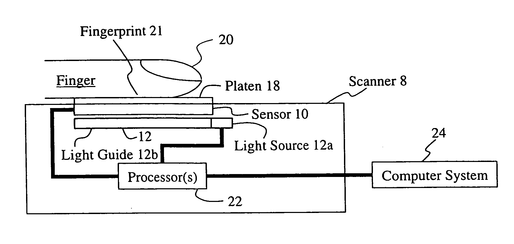
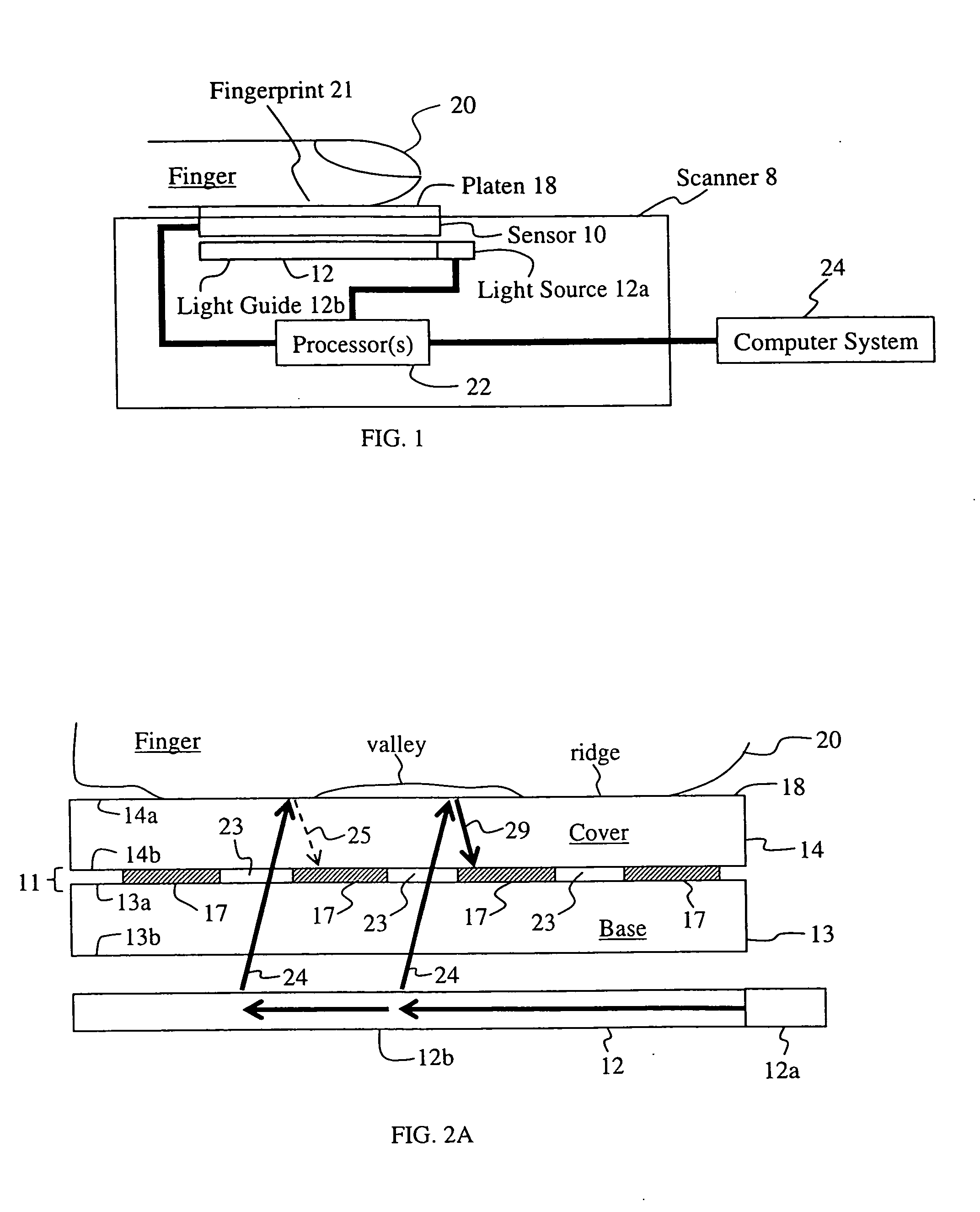
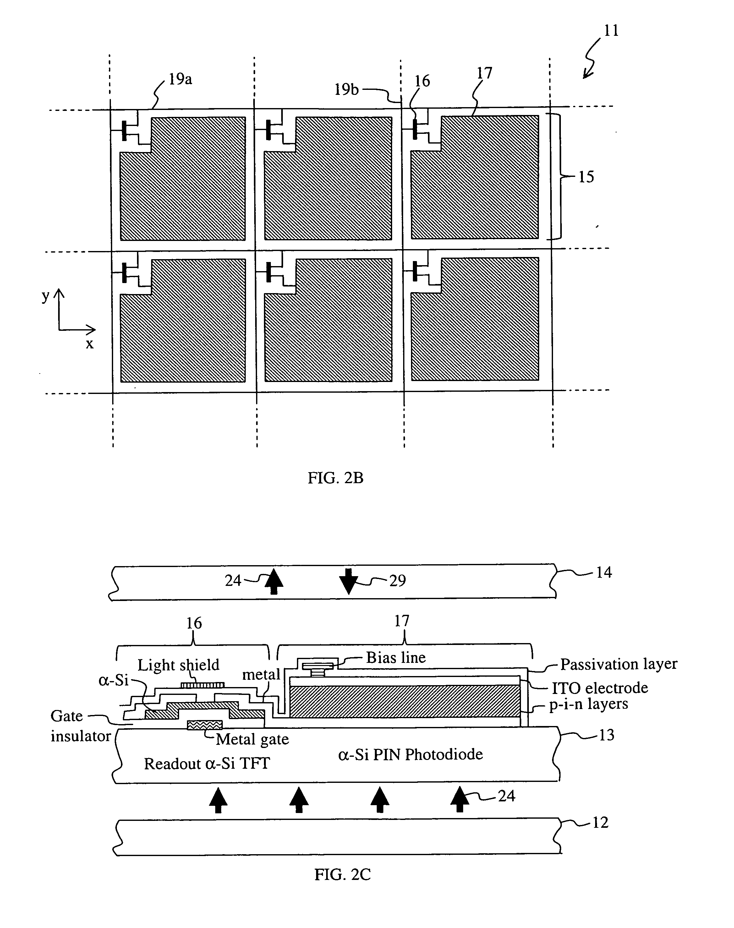
[0029]Referring to FIG. 1, a block diagram of a scanner 8 for capturing fingerprints of one or more fingers (with or without thumb) using a sensor 10 of the present invention is shown. FIG. 1 shows an illuminator 12 for transmitting light to sensor 10. Illuminator 12 may be provided by light source(s) 12a, such as LED(s) providing illumination to a light guide or panel 12b which then directs such illumination towards sensor 10. The sensor 10 is an assembly of a first substrate or base 13 upon which is formed a two-dimensional (2D) array 11 (FIG. 2B) of pixel elements (or pixels) 15 as each location along the array, and a second substrate or cover 14. As shown in FIG. 2A, base 13 has upper surface 13a and a lower surface 13b, and the array 11 are formed on a upper surface 13a, and cover 14 has an upper surface 14a opposite base 13. As will be discuss later in FIG. 4, the base 13 and cover 14 may switch positions, whereby surfaces 13b and 13a are the upper and lower surfaces of base 1...


PUM


Abstract

A sensor for detecting fingerprints is provided having first and second substrates, a two-dimensional array of sensing elements formed on the first substrate, and a plurality of thin-film transistors or TFTs for controlling the sensing elements at pixel location along the array. Each of the sensing elements detects one of electrical signals (e.g., capacitance, resistance, or impedance), temperature, or light via one of the first or second substrates representative of one or more fingerprints. The top of the second substrate or the bottom of the first substrate may provide a platen upon which one or more fingers can be disposed. The sensor may be utilized in a fingerprint scanner having one or more processors driving sensing elements or reading from sensing elements analog signals representative of one or more fingerprints, and generating an image representative of the one or more fingerprints from the analog signals.

Description

[0001]This application claims the benefit of priority to U.S. Provisional Patent Application No. 61 / 486,766, filed May 17, 2011, which is herein incorporated by reference.FIELD OF THE INVENTION[0002]The present invention relates to sensors, methods, and systems for detecting one or more fingerprints, and particularly a sensor for detecting one or more fingerprints utilizing thin-film transistors (TFT). The present invention is particularly useful in providing a fingerprint sensor having sensing element(s) at each pixel location of a two-dimension array where sensing element(s) are coupled to one a TFT at the pixel location for use in a fingerprint scanner to provide a two-dimension fingerprint image of one or more fingers. At each pixel location, a single sensing element of desired type or characteristic (e.g., light, electrical, or thermal sensing) may be coupled to a TFT enabling driving and readout of the sensing element, or multiple sensing elements of the same or different type...

Claims


Application Information

Patent Timeline
Patent Type & Authority Applications(United States)
IPC IPC(8): G06K9/00G06V30/144
CPCG06K9/0004G06K9/00013G06K9/00046G06K9/0012G06V40/1324G06V40/1318G06V40/1394
Inventor CARVER, JOHN F.RAGUIN, DANIEL H.
Owner CROSS MATCH TECH
Why Eureka
Try Eureka