

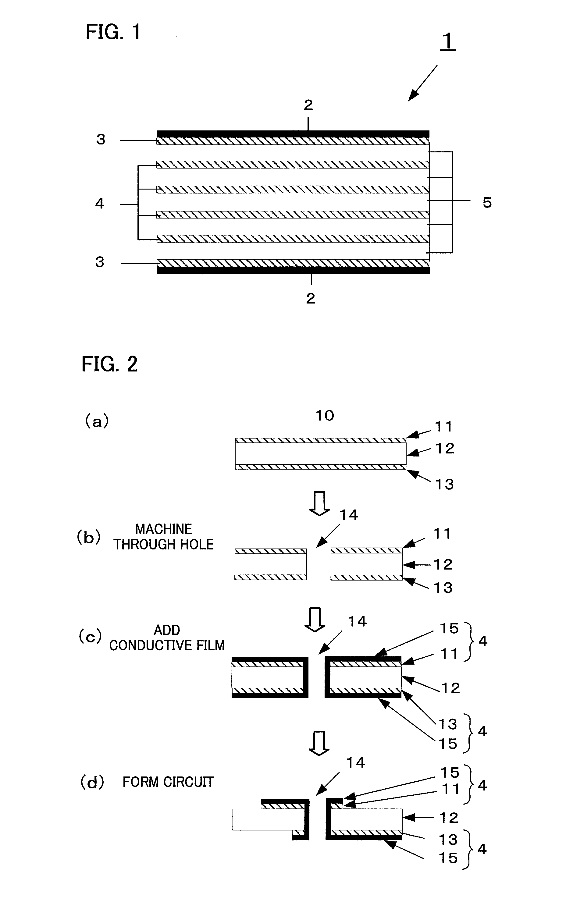
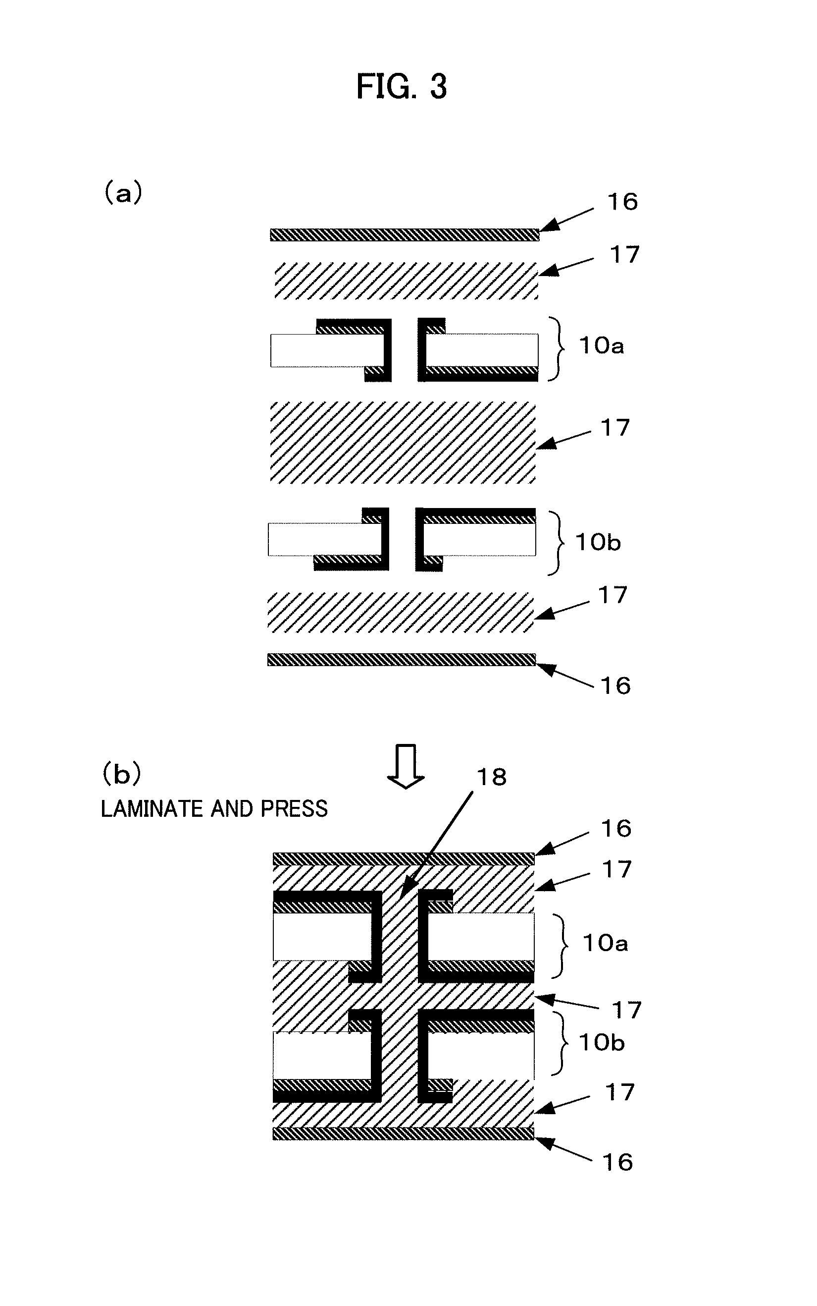
Printed wiring board with improved corrosion resistance and yield
- Summary
- Abstract
- Description
- Claims
- Application Information
AI Technical Summary
Benefits of technology
Problems solved by technology
Method used
Image

Examples
first embodiment
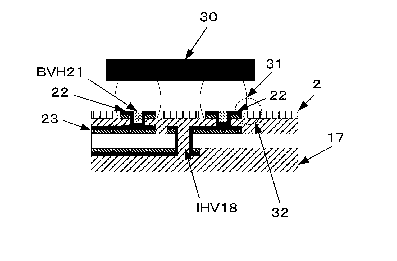
[0035]FIG. 5 is a diagram for explaining the printed wiring board 1 according to the present invention.
[0036]The pads 22 for mounting a ball grid array part 30 as electronic part on the printed wiring board 1 is formed, as part of the desired circuit pattern of the surface conductive layer 3, in the printed wiring board 1. The ball grid array part 30 is a surface-mount package in which a solder ball terminal 31 for jointing terminals is formed on the bottom of the package in a grid shape. The solder ball terminals 31 of the ball grid array part 30 and the pads 22 provided on the printed wiring board are joined with each other by melting the solder ball terminals 31, and thus the ball grid array part 30 is electrically and mechanically joined to the printed wiring board 1.
[0037]In the first embodiment, the pads 22 and the inner conductive layers 4 of the copper-laminated plates 10 therebelow are electrically connected through the blind via holes (BVH) 21. Thereby, the wires leading f...
second embodiment
[0039]FIG. 6 is a diagram for explaining a printed wiring board 1 according to the present invention.
[0040]The printed wiring board 1 is such that the copper-laminated plates 10 and the prepregs 17 are alternately laminated and the surface conductive layers 3 are provided at the outermost positions outside the prepregs 17. The printed wiring board 1 has the individually-formed pads 22 for surface-mount parts to be mounted on the surface of the printed wiring board 1, and at least one solid pattern 33 including two or more pads and formed to be connected or filled with pattern width larger than the minimum width of the pads. The pads 22 and the solid pattern 33 are circuit-formed on the surface conductive layer 3.
[0041]The printed wiring board 1 according to the second embodiment is configured such that all the leading wires from the pads 22 not included in the solid pattern 33 are connected to the inner conductive layers 4 of the copper-laminated plates 10 through the blind via hole...
PUM
 Abstract
Description
Claims
Application Information