Fabrication of graphene nanoelectronic devices on soi structures

a technology of nanoelectronic devices and graphene nanoelectronic devices, which is applied in the direction of semiconductor devices, basic electric elements, electrical apparatus, etc., can solve the problems of difficult integration with other circuit components, and the integration of graphene devices and silicon devices has not been realized

Active Publication Date: 2013-01-03
GLOBALFOUNDRIES U S INC
View PDF6 Cites 14 Cited by
  • Summary
  • Abstract
  • Description
  • Claims
  • Application Information

AI Technical Summary

Benefits of technology

[0009]Embodiments of the invention provide a method to fabricate graphene devices and / or test structures by using an SOI wafer with built-in contact areas. Instead of using metals, highly doped SOI is used to make contact to graphene channel. This metal-less contact scheme eliminates the thermal budget limitations associated with metal contacts. Undoped SOI is used in embodiments of the invention to provide the ideal platform for graphene and Si hybrid circuits. Since the oxide substrate is found to cause significant noise and mobility degradation in most of the graphene devices studied so far, SOI may provide a better substrate to achieve low-noise, high performance graphene devices.

Problems solved by technology

Most graphene devices considered and studied so for are fabricated on an oxide substrate, which makes it difficult to integrate with other circuit components.
So far, the integration of graphene devices and silicon devices has not been realized.

Method used


Image

  • Fabrication of graphene nanoelectronic devices on soi structures
  • Fabrication of graphene nanoelectronic devices on soi structures
  • Fabrication of graphene nanoelectronic devices on soi structures

Examples


Embodiment Construction

[0034]In the following description, numerous specific details are set forth, such as particular structures, components, materials, dimensions, processing steps and techniques, in order to provide a thorough understanding of the present invention. However, it will be appreciated by one of ordinary skill in the art that the invention may be practiced with a wide range of specific details. In other instances, well-known structures or processing steps have not been described in detail in order to avoid obscuring the invention.

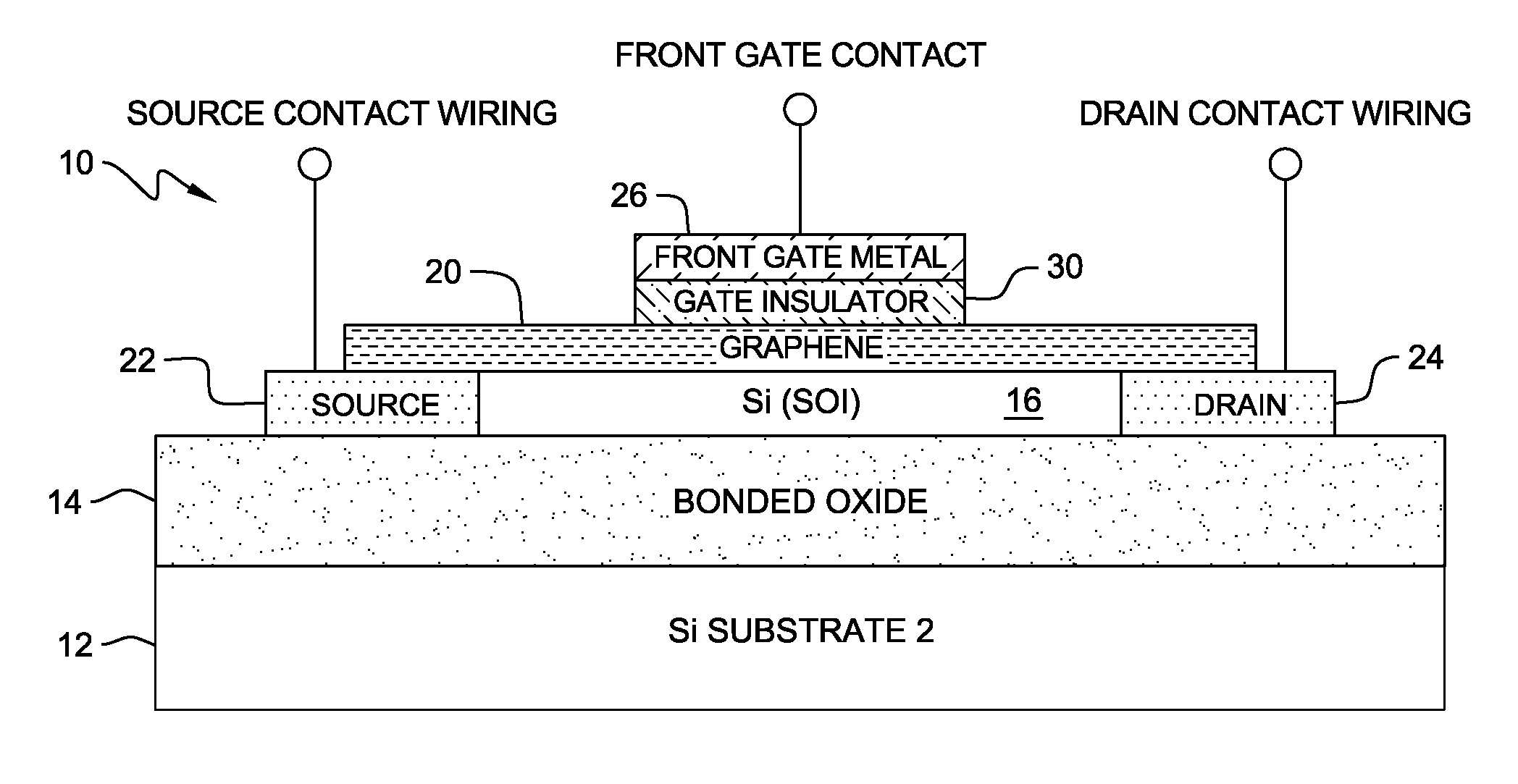
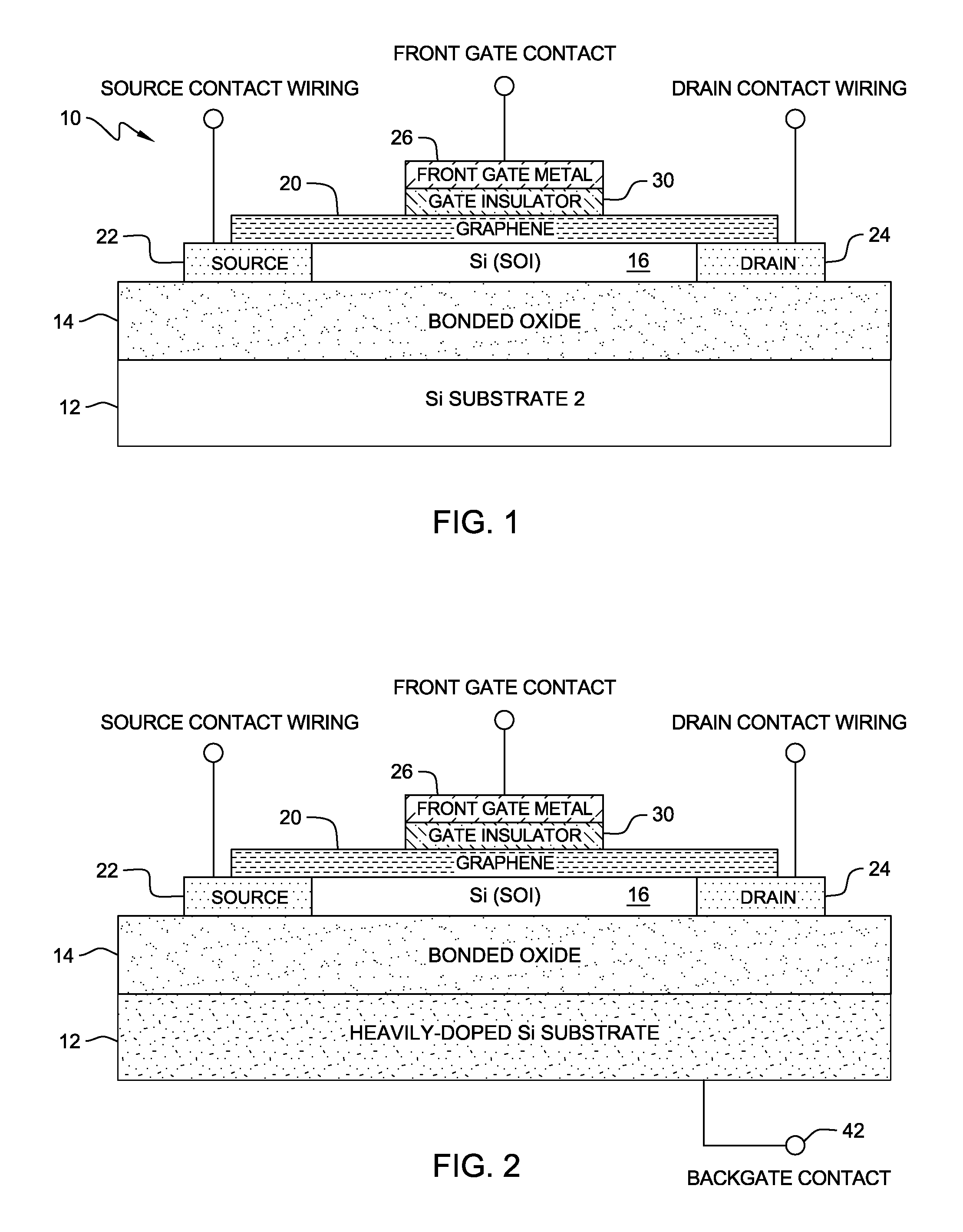
[0035]FIG. 1 shows a cross-sectional view of an example graphene electronic device fabricated on a silicon-on-insulator (SOI) structure according to one embodiment of the present invention. Structure 10 comprises a base semiconductor substrate 12, an insulator layer 14, a semiconductor layer 16, graphene layer 20, source region 22, drain region 24, front gate metal 26, and gate insulator 30.

[0036]The base semiconductor substrate layer 12 may comprise any semiconduc...


PUM

PropertyMeasurementUnit
thicknessaaaaaaaaaa
thicknessaaaaaaaaaa
thicknessaaaaaaaaaa

Abstract

A semiconductor-on-insulator structure and a method of forming the silicon-on-insulator structure including an integrated graphene layer are disclosed. In an embodiment, the method comprises processing a silicon material to form a buried oxide layer within the silicon material, a silicon substrate below the buried oxide, and a silicon-on-insulator layer on the buried oxide. A graphene layer is transferred onto the silicon-on-insulator layer. Source and drain regions are formed in the silicon-on-insulator layer, and a gate is formed above the graphene. In one embodiment, the processing includes growing a respective oxide layer on each of first and second silicon sections, and joining these silicon sections together via the oxide layers to form the silicon material. The processing, in an embodiment, further includes removing a portion of the first silicon section, leaving a residual silicon layer on the bonded oxide, and the graphene layer is positioned on this residual silicon layer.

Description

CROSS REFERENCE TO RELATED APPLICATION[0001]This application is a divisional application of copending U.S. patent application Ser. No. 12 / 620,320, filed Nov. 17, 2009, the entire content and disclosure of which is hereby incorporated herein by reference.BACKGROUND OF THE INVENTION[0002]1. Field of the Invention[0003]This invention generally relates to semiconductor-on-insulator structures, and more specifically, to silicon-on-insulator structures having graphene nanoelectronic devices.[0004]2. Background Art[0005]Semiconductor-on-insulator (SOI) technology is becoming increasingly important in semiconductor processing. An SOI substrate structure typically contains a buried insulator layer, which functions to electrically isolate a top semiconductor device layer from a base semiconductor substrate. Active devices, such as transistors, are typically formed in the top semiconductor device layer of the SOI substrate. Devices formed using SOI technology (i.e., SOI devices) offer many adv...

Claims


Application Information

Patent Timeline
Patent Type & Authority Applications(United States)
IPC IPC(8): H01L29/78H01L29/165H01L29/08
CPCH01L29/1606H01L29/78687H01L29/7781H01L29/66742
Inventor LIN, YU-MINGYAU, JENG-BANG
Owner GLOBALFOUNDRIES U S INC
Why Eureka
Try Eureka