Fabrication of graphene nanoelectronic devices on SOI structures
- Summary
- Abstract
- Description
- Claims
- Application Information
AI Technical Summary
Benefits of technology
Problems solved by technology
Method used
Image
Examples
Embodiment Construction
[0033]In the following description, numerous specific details are set forth, such as particular structures, components, materials, dimensions, processing steps and techniques, in order to provide a thorough understanding of the present invention. However, it will be appreciated by one of ordinary skill in the art that the invention may be practiced with a wide range of specific details. In other instances, well-known structures or processing steps have not been described in detail in order to avoid obscuring the invention.
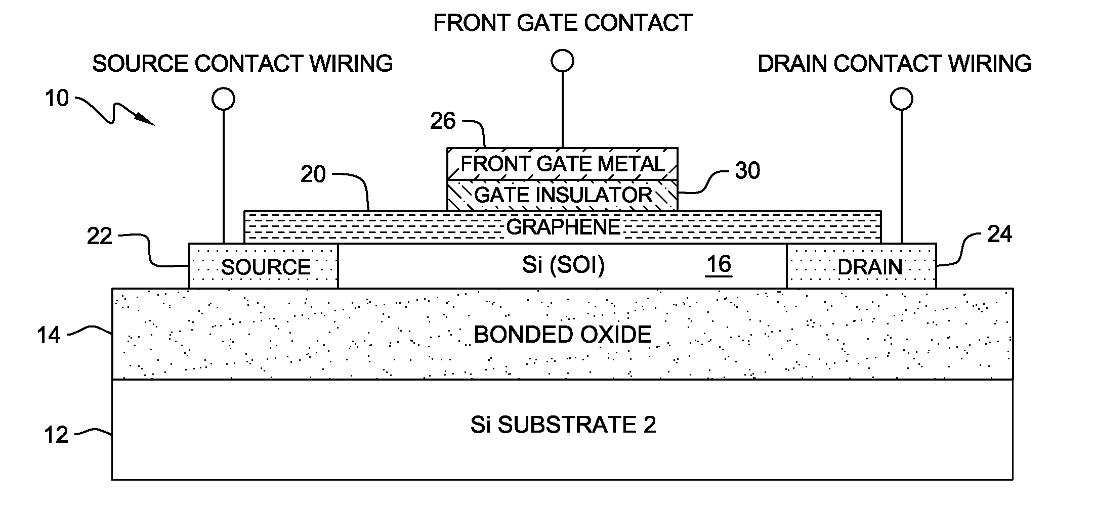
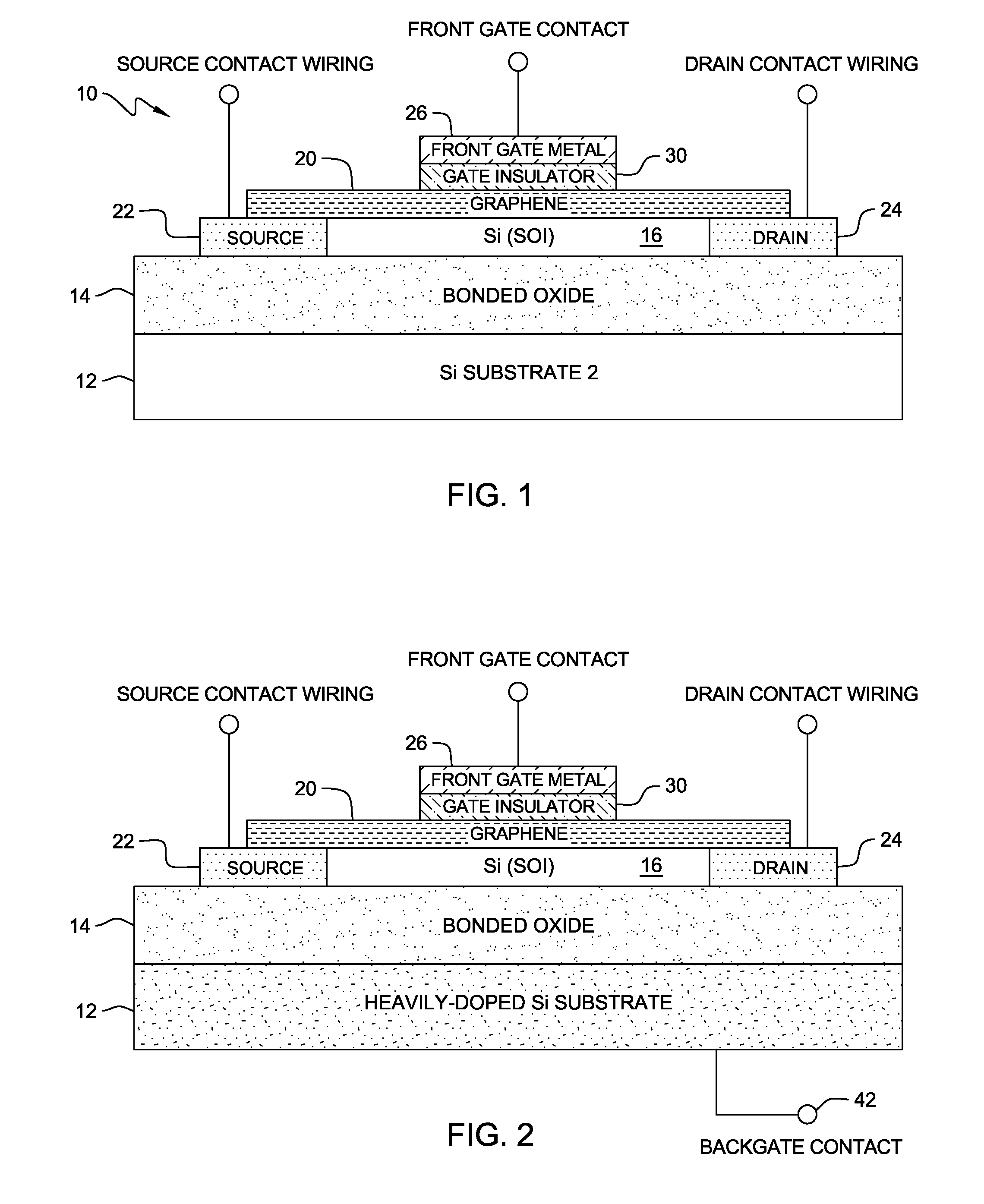
[0034]FIG. 1 shows a cross-sectional view of an example graphene electronic device fabricated on a silicon-on-insulator (SOI) structure according to one embodiment of the present invention. Structure 10 comprises a base semiconductor substrate 12, an insulator layer 14, a semiconductor layer 16, graphene layer 20, source region 22, drain region 24, front gate metal 26, and gate insulator 30.
[0035]The base semiconductor substrate layer 12 may comprise any semiconduc...
PUM
 Abstract
Description
Claims
Application Information


