Semiconductor structure and method for manufacturing the same

a semiconductor and structure technology, applied in the direction of semiconductor devices, semiconductor/solid-state device details, electrical apparatus, etc., can solve the problems of reducing the contact resistance of the source/drain region, affecting the production efficiency of semiconductor products, so as to reduce the leakage current, reduce the eor defect, and reduce the contact resistance

Active Publication Date: 2013-01-03
INST OF MICROELECTRONICS CHINESE ACAD OF SCI
View PDF1 Cites 50 Cited by
  • Summary
  • Abstract
  • Description
  • Claims
  • Application Information

AI Technical Summary

Benefits of technology

[0012]The object of the present invention is to provide a semiconductor structure and a method for manufacturing the same, which are beneficial to the reduction the contact resistance.
[0027]As compared with the prior art, the present invention has the following advantages:
[0028]The exposed part of the source / drain region comprises the bottom and the sidewalls by etching the source / drain region, which increases the contact area between the contact metal and the source / drain region in the contact hole, and reduces the contact resistance. This invention conformally forms an amorphous layer on the exposed part of the source / drain region, instead of forming the amorphous substance by amorphous ion implantation, as a result, it is beneficial to the reduction of EOR defects caused by the amorphous ion implantation and thus reduce the leakage current.

Problems solved by technology

However, although the above method can decrease the contact resistance of the source / drain region, quite a few defects may be caused by performing the ion implantation and then the annealing during the decrystallizatoin process.
These EOR defects seriously deteriorate the electrical properties, especially the carrier mobility of the substrates, and as a result, it is unsuitable to manufacture electronic elements with these substrates.
Therefore, under the tendency that the semiconductor device size becomes smaller, it becomes a problem urgently to be solved to effectively increase the contact area of the semiconductor while reducing the contact resistance.

Method used


Image

  • Semiconductor structure and method for manufacturing the same
  • Semiconductor structure and method for manufacturing the same
  • Semiconductor structure and method for manufacturing the same

Examples


Embodiment Construction

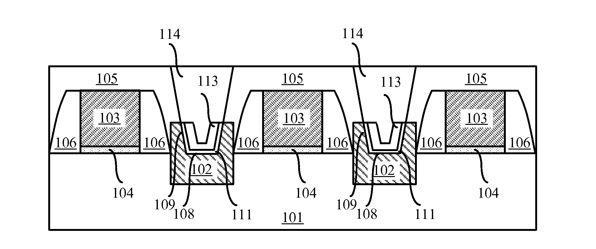
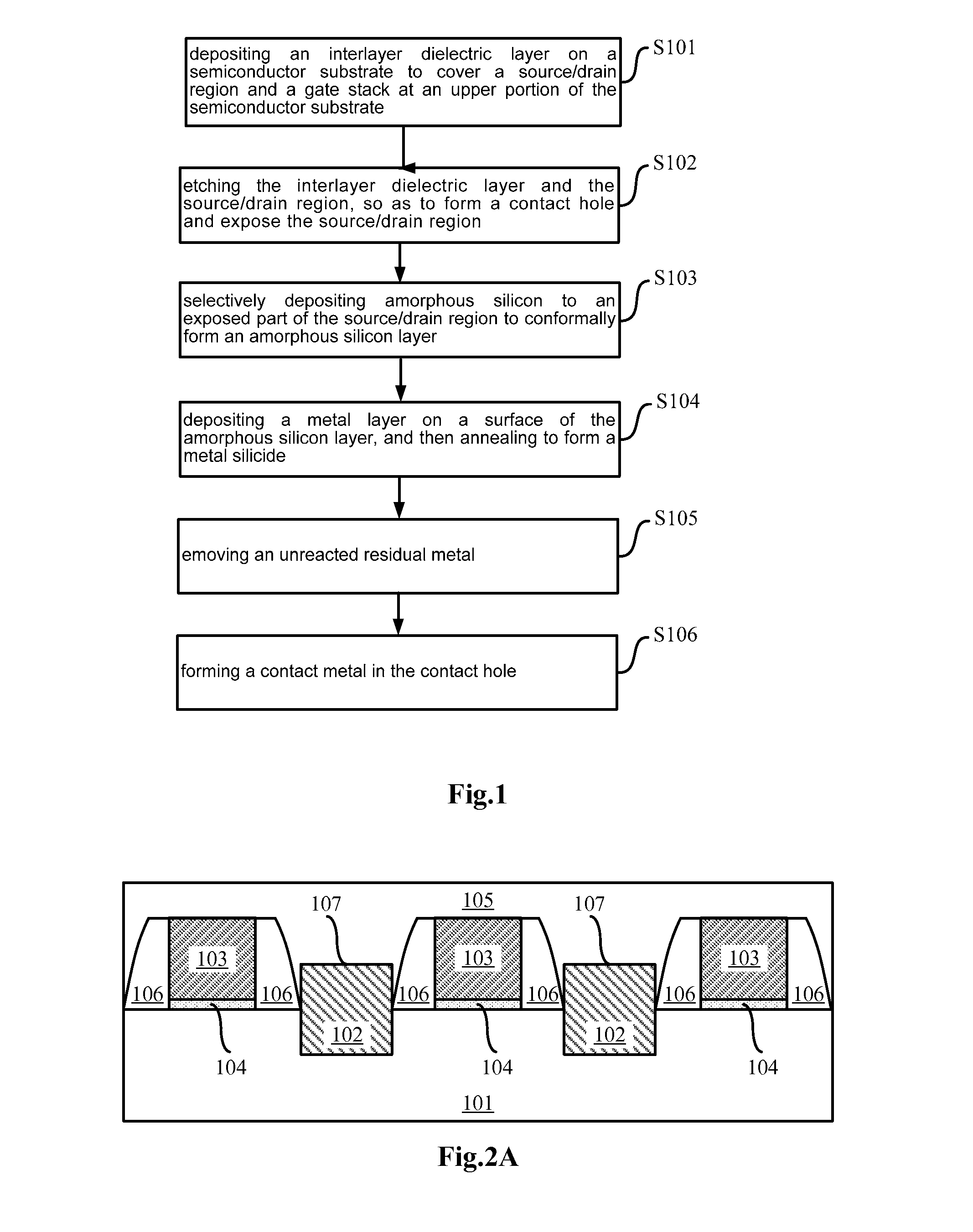
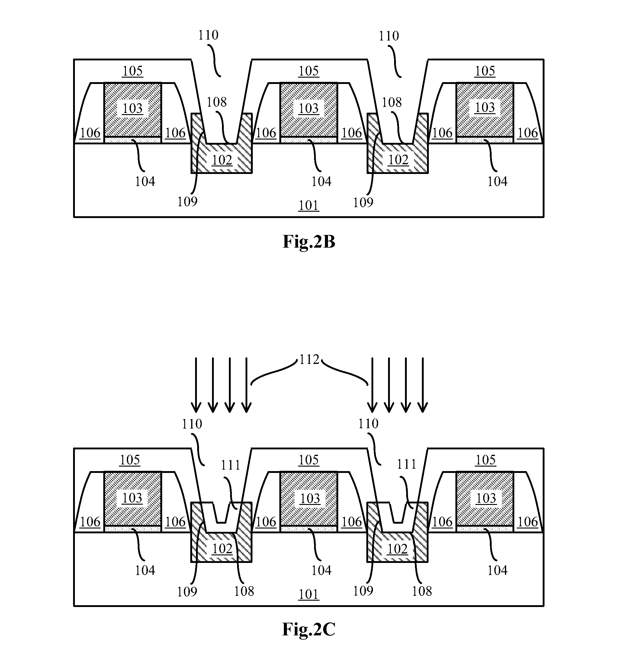
[0033]The embodiments of the present invention are described in detail as follows. The examples of the embodiments are illustrated in the drawings, throughout which the same or similar reference signs represent the same or similar elements or elements having the same or similar functions. The embodiments described as follows with reference to the drawings are exemplary, and are merely used to interpret the present invention, rather than limiting the present invention.

[0034]The following disclosure provides many different embodiments or examples to implement different structures of the present invention. In order to simplify the disclosure of the present invention, the components and arrangements of specific examples are described in the following text. Apparently, they are just exemplary, and do not intend to restrict the present invention. In addition, reference numbers and / or letters can be repeatedly used in different examples of the present invention for the purposes of simplifi...


PUM

PropertyMeasurementUnit
thicknessaaaaaaaaaa
thicknessaaaaaaaaaa
thicknessaaaaaaaaaa

Abstract

The present invention provides a method for manufacturing a semiconductor structure, comprising the steps of: depositing an interlayer dielectric layer (105) on a semiconductor substrate (101) to cover a source / drain region (102) and a gate stack on the semiconductor substrate (101); etching the interlayer dielectric layer and the source / drain region, so as to form a contact hole (110) extending into the source / drain region; conformally forming an amorphous layer (111) on an exposed part of the source / drain region; forming a metal silicide layer (113) on a surface of the amorphous layer (111); and filling the contact hole (110) with a contact metal (114). Correspondingly, the present invention further provides a semiconductor structure. The present invention etches the source / drain region so that the exposed part comprises the bottom and a sidewall, thereby expanding the contact area between the contact metal in the contact hole and the source / drain region, and reducing the contact resistance. The present invention effectively eliminates EOR defects caused by the amorphous ion implantation by forming an amorphous substance by a selective deposition.

Description

[0001]This application claims priority to a Chinese patent application No. 201010296962.8, filed on Sep. 29, 2010, entitled “semiconductor structure and method for manufacturing the same”, which is hereby incorporated by reference in its entirety.FIELD OF THE INVENTION[0002]This invention relates to a technology of semiconductor manufacturing, and particularly to a semiconductor structure and a method for manufacturing the same.BACKGROUND OF THE INVENTION[0003]With the development of the semiconductor industry, integrated circuits with higher performances and stronger functions require a larger element density. In addition, the sizes of various components / elements or the spaces between them need to be further reduced. Accordingly, the contact area between the source / drain region and the metal electrode is decreased. As the contact resistivity between the contact surfaces of the conventional source / drain region and the metal electrode is larger, such decreased contact area causes an ...

Claims


Application Information

Patent Timeline
Patent Type & Authority Applications(United States)
IPC IPC(8): H01L29/78H01L21/336
CPCH01L21/28518H01L21/28525H01L2924/0002H01L21/76805H01L21/823425H01L21/823807H01L21/823814H01L21/823871H01L23/485H01L29/41725H01L29/41783H01L29/517H01L29/518H01L29/66628H01L29/66636H01L29/7848H01L2924/00
Inventor YIN, HAIZHOULUO, ZHIJIONGZHU, HUILONG
Owner INST OF MICROELECTRONICS CHINESE ACAD OF SCI
Why Eureka
Try Eureka