Multilayer printed circuit board and manufacturing method therefor

a printed circuit board and multi-layer technology, applied in the direction of conductive pattern formation, electrical apparatus construction details, semiconductor/solid-state device details, etc., can solve the problem of even more difficult size reduction of the board b>100/b>, and achieve the effect of reducing the manufacturing cost of the board

Inactive Publication Date: 2013-01-03
SANYO ELECTRIC CO LTD
View PDF11 Cites 37 Cited by
  • Summary
  • Abstract
  • Description
  • Claims
  • Application Information

AI Technical Summary

Benefits of technology

[0017]Furthermore, a manufacturing cost for the board is reduced because steps required for providing connection means that pen...

Problems solved by technology

In such a case, a size reduction ...

Method used


Image

  • Multilayer printed circuit board and manufacturing method therefor
  • Multilayer printed circuit board and manufacturing method therefor
  • Multilayer printed circuit board and manufacturing method therefor

Examples


Embodiment Construction

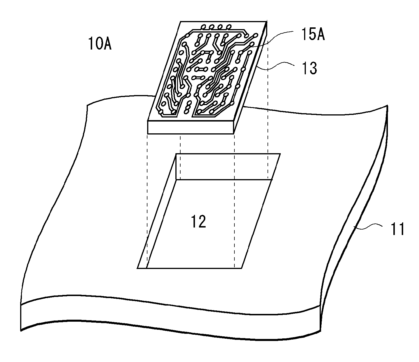
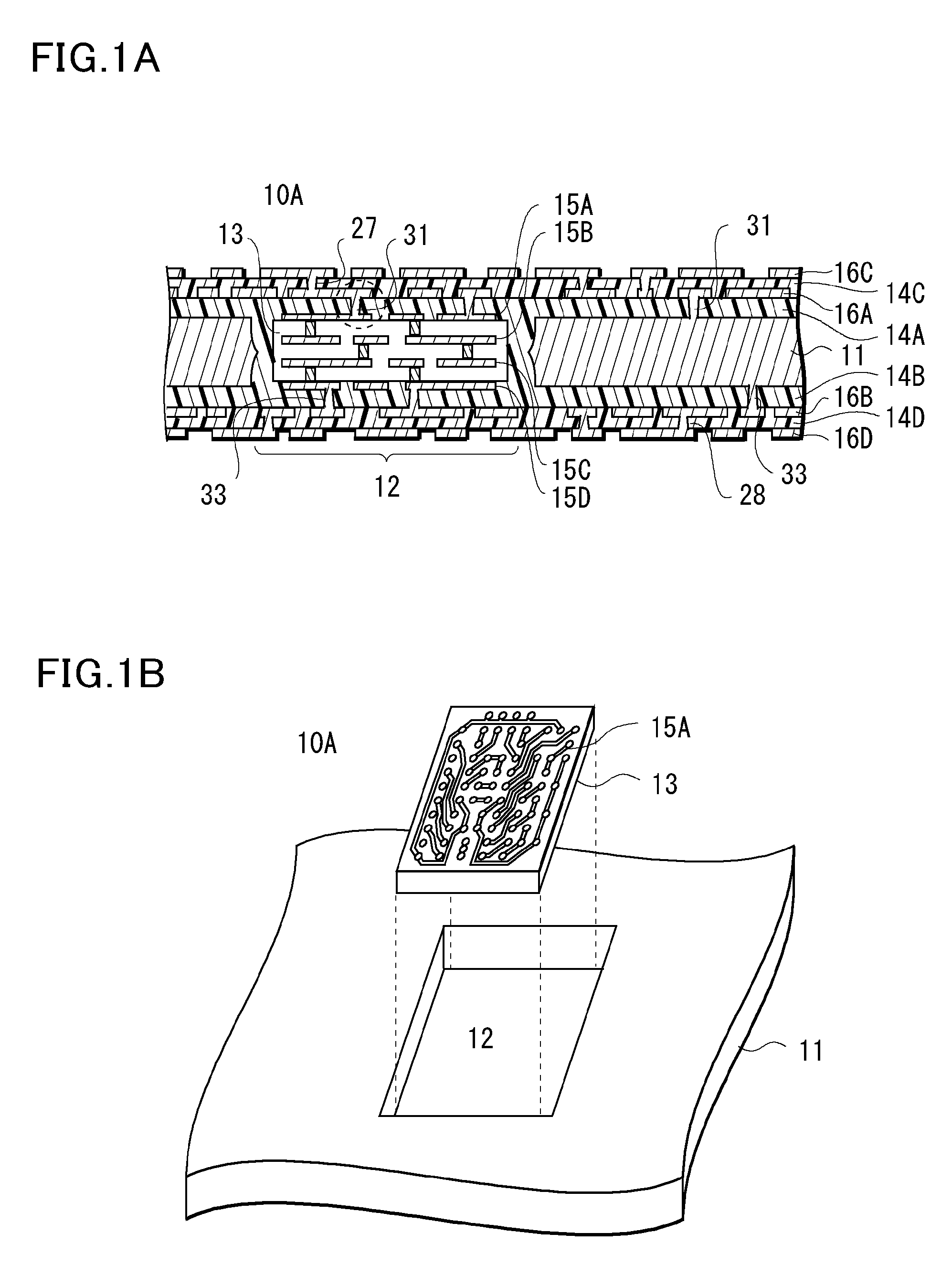
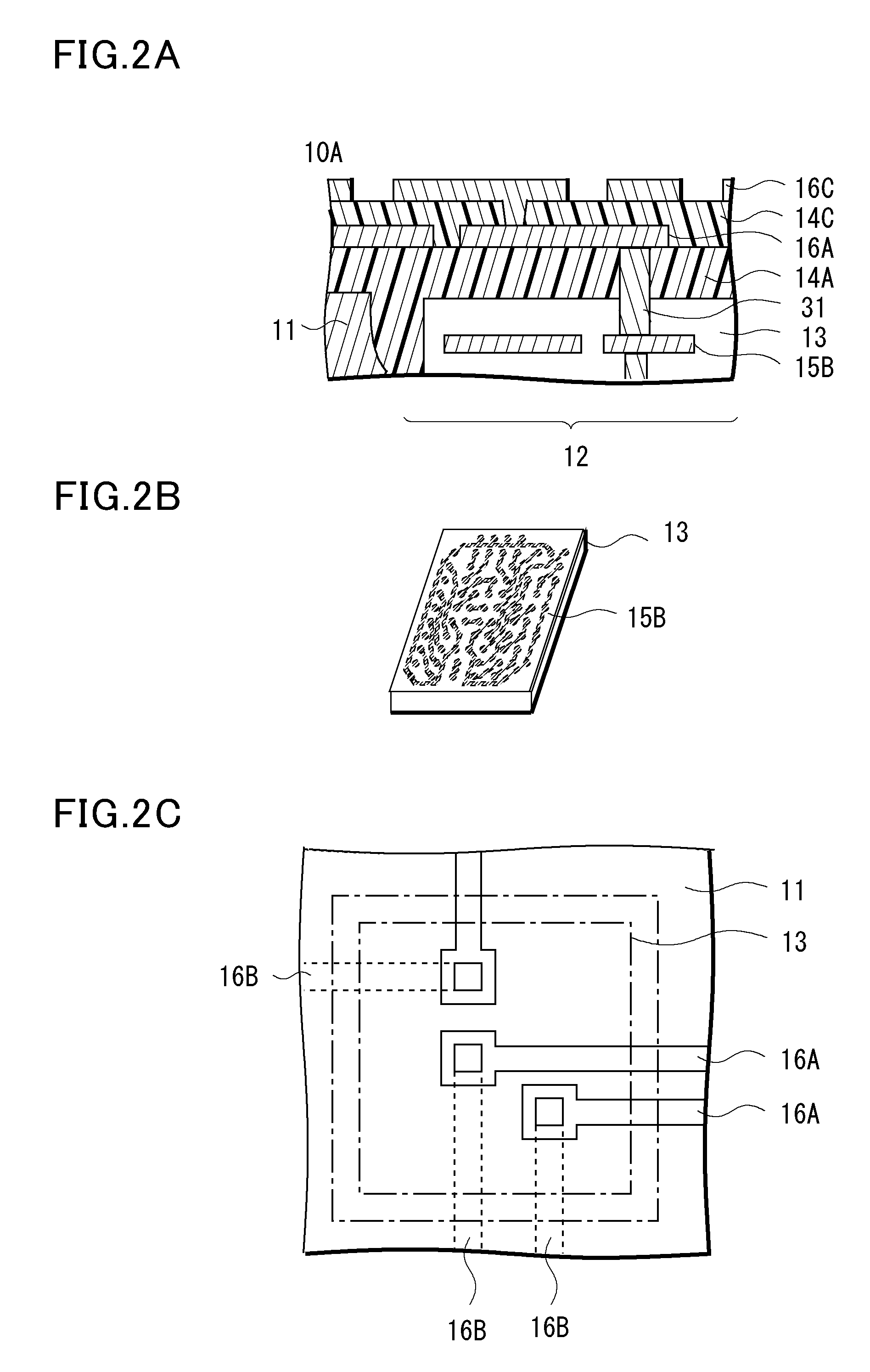
[0027]Referring to FIG. 1, the configuration of a board 10A of the present embodiment is described. FIG. 1A is a sectional view showing the configuration of the board 10A, and FIG. 1B is a perspective view schematically showing the board 10A.

[0028]Referring to FIG. 1A, the board 10A includes a thick core layer 11, wiring layers (a first wiring layer 16A and a third wiring layer 16C) stacked on an upper surface of the core layer 11 with insulating layers interposed, wiring layers (a second wiring layer 16B and a fourth wiring layer 16D) stacked on a lower surface of the core layer 11 with insulating layers interposed, and a connection board 13 embedded in a removed area 12 of the core layer 11.

[0029]Although multilayered wiring having a total of four layers is formed on the upper and lower main surfaces of the core layer 11 here, the number of the wiring layers to be stacked is not limited to four layers. Two wiring layers or six or more wiring layers may be formed.

[0030]The core lay...


PUM

PropertyMeasurementUnit
Currentaaaaaaaaaa
Currentaaaaaaaaaa
Digital informationaaaaaaaaaa

Abstract

Provided is a substrate wherein wiring layers laminated onto the top and bottom surfaces of a core layer are connected to each other by a simple means. Also provided is a method for manufacturing said substrate. In the provided substrate (10A), a connection substrate (13) is placed in a removed region (12) which goes all the way through a part of a thick core layer (11). Said connection substrate (13) electrically connects a first wiring layer (16A) laminated onto the top surface of the core layer (11) to a second wiring layer (16B) laminated onto the bottom surface of the core layer (11). This eliminates the requirement of providing a through-hole through the core layer (11) for each connection, resulting in a small form-factor substrate (10A) with a high wiring density.

Description

REFERENCE TO RELATED APPLICATIONS[0001]This application is a national stage application under 35 USC 371 of International Application No. PCT / JP2011 / 054420, filed Feb. 21, 2011, which claims the priority of Japanese Patent Application No. 2010-36239, filed Feb. 22, 2010, and Japanese Patent Application No. 2011-028582, filed Feb. 14, 2011, the entire contents of which are incorporated herein by reference.FIELD OF THE INVENTION[0002]The present invention relates to a multilayer printed circuit board and a method of manufacturing the same, and particularly relates to a multilayer printed circuit board and a method of manufacturing the same, in which a multilayered wiring layer is stacked on both an upper surface and a lower surface of a core layer.BACKGROUND OF THE INVENTION[0003]Recent electronic devices offer higher performances and are smaller in size than before, and the significance of heat dissipation has been elevated by an increase in the capacities of components mounted on a ...

Claims


Application Information

Patent Timeline
IPC IPC(8): H05K1/03H05K3/10H05K7/06
CPCH05K1/185H05K3/4608H05K2201/10378H05K2203/063H05K2203/1469Y10T29/49162H01L24/19H01L2224/16225H01L2924/15311H01L2924/19105H01L23/5389H01L2224/04105H01L2924/12042H01L2924/15787H01L2924/15788H01L2924/00
Inventor IGARASHI, YUSUKENAKAMURA, TAKESHI
Owner SANYO ELECTRIC CO LTD
Why Eureka
Try Eureka