Electronic device, wiring board, and method of shielding noise

a technology of electronic devices and wiring boards, applied in the direction of cross-talk/noise/interference reduction, electrical apparatus construction details, printed capacitor incorporation, etc., can solve the problems of inadequate countermeasures and need to consider the leakage of noise from gaps, so as to prevent the leakage of noise propagating

Active Publication Date: 2013-01-03
NEC CORP
View PDF2 Cites 17 Cited by
  • Summary
  • Abstract
  • Description
  • Claims
  • Application Information

AI Technical Summary

Benefits of technology

[0012]Furthermore, according to the present invention, there is provided a method of shielding a noise that is used for shielding the noise that is generated by an electronic component mounted on one face of a wiring board including: shielding a noise propagating from the electronic component to the air using a metal cap that covers the electronic component; shielding a noise propagating above the surface of one face using a first conductive body that is located on the one face, is arranged so as to surround the electronic component, and is connected to an end portion of the metal cap; shielding a noise propagating between a second conductive body that is located in a first layer, is connected to the electronic component through a first connection member, and has a gap and a third conductive body that is located in a second layer facing the one face through

Problems solved by technology

In addition, in a case where there is a hole or a gap in the parallel flat plates, the leakage of noise from the gap needs to be considered.
Thus,

Method used


Image

  • Electronic device, wiring board, and method of shielding noise
  • Electronic device, wiring board, and method of shielding noise
  • Electronic device, wiring board, and method of shielding noise

Examples


first embodiment

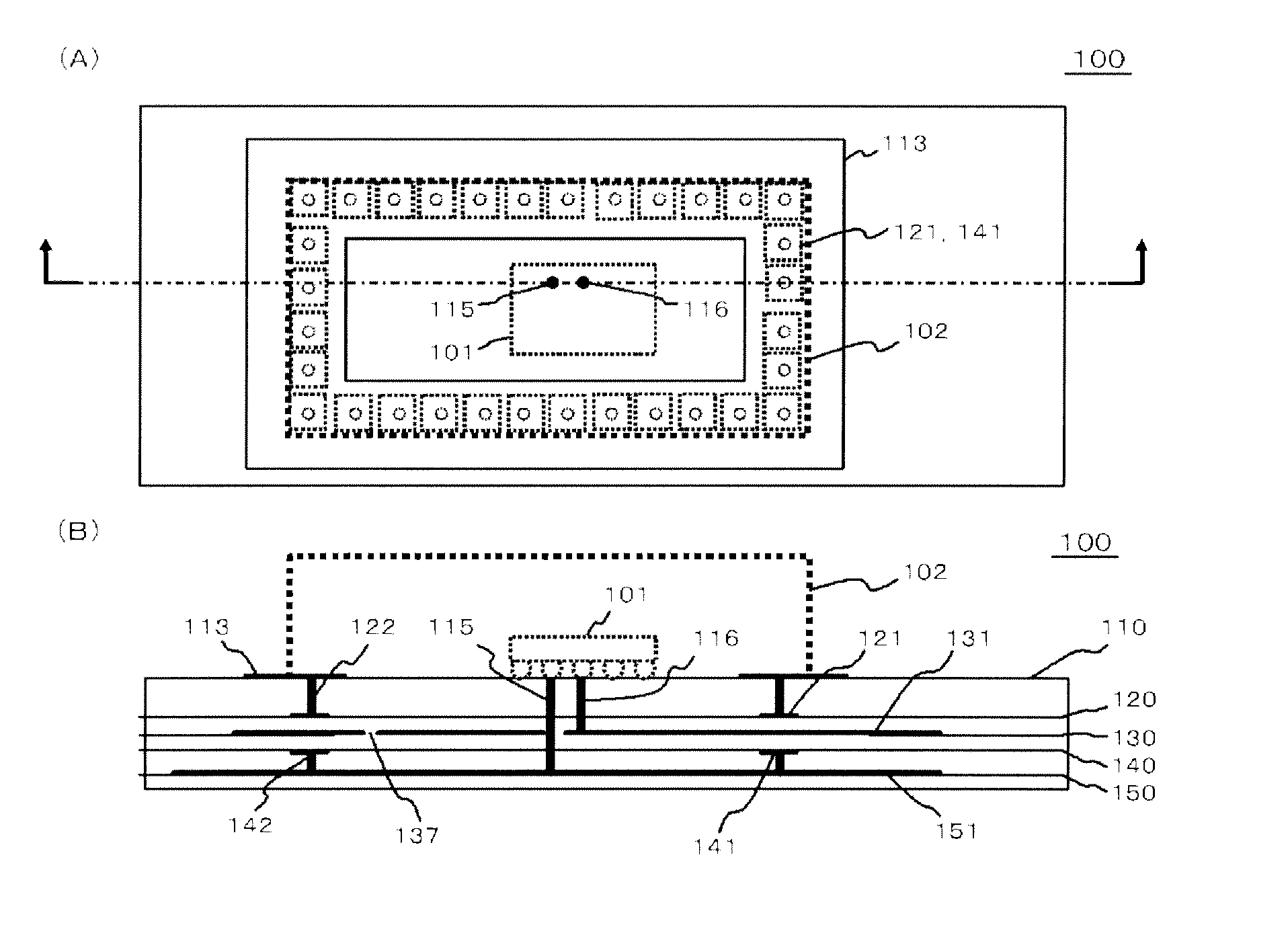
[0033]FIG. 1 represents a top view and a cross-sectional view of a wiring board 100 according to a first embodiment of the present invention. Described in more detail, FIG. 1(A) is a top view of the wiring board 100, and FIG. 1(B) is a cross-sectional view of the wiring board 100 that is taken along a cross-section line represented in FIG. 1(A). The wiring board 100 is a multi-layer board that includes at least an A layer 110, a B layer 120, a C layer 130, a D layer 140, and an E layer 150 facing one another. In addition, the wiring board 100 may further include a layer other than the above-described five layers. For example, a dielectric layer may be located between the layers. Furthermore, the wiring board 100 may further include a hole, a via, or the like that is not shown in the diagrams in a range not contradicting the configuration of the present invention. In addition, in the above-described five layers, signal lines may be arranged in a range not contradicting the configurat...

second embodiment

[0060]FIG. 6 represents a top view and a cross-sectional view of an electronic device 200 according to a second embodiment of the present invention. Described in more detail, FIG. 6(A) is a top view of the electronic device 200, and FIG. 6(B) is a cross-sectional view of an electronic device 200 that is taken along a cross-section line represented in FIG. 6(A). The electronic device 200 is a multi-layer board that includes at least an A layer 210, a B layer 220, a C layer 230, a D layer 240, an E layer 250, and an F layer 260, and a G layer 270 facing one another. In addition, the electronic device 200 may further include a layer other than the above-described seven layers. For example, a dielectric layer may be located between the layers. Furthermore, the electronic device 200 may further include a hole, a via, or the like that is not shown in the diagrams in a range not contradicting the configuration of the present invention. In addition, in the above-described seven layers, sign...

third embodiment

[0102]FIG. 16 represents a top view and a cross-sectional view of an electronic device 200 according to a third embodiment of the present invention. Described in more detail, FIG. 16(A) is a top view of the electronic device 200, and FIG. 16(B) is a cross-sectional view of the electronic device 200 that is taken along a cross-section line represented in FIG. 16(A). The electronic device 200 of this embodiment has a configuration that is acquired by adding an H layer 280 to the electronic device 200 described in the second embodiment. The constituent elements included in the A layer 210, the B layer 220, the C layer 230, the D layer 240, the E layer 250, the F layer 260, and the G layer 270 are similar to those of the second embodiment, and the detailed description thereof will not be presented.

[0103]FIG. 17 is a diagram that illustrates the H layer 280 of the electronic device 200. The H layer 280 (third layer) is located between the A layer 210 and the B layer 220 and faces the G l...


PUM


Abstract

A wiring board includes a metal cap pad that is arranged so as to surround a mounting position of an electronic component and is connected to an end portion of a metal cap, a power source plane that is connected to the electronic component through a connection member and has a gap, a ground plane that is connected to the electronic component through a connection member, and a plurality of conductive body elements that are repeatedly arranged so as to surround the connection members and the gap. The power source plane and the ground plane extend so as to include at least a part of an area that is surrounded by the plurality of conductive body elements and at least a part of an area facing the plurality of conductive body elements.

Description

TECHNICAL FIELD[0001]The present invention relates to an electronic device, a wiring board, and a method of shielding a noise.BACKGROUND ART[0002]In an electronic device, there are cases where a noise generated from an electronic component propagates through a parallel flat plane that is formed by a power source-ground plane as a kind of a waveguide so as to have an adverse influence on the other electronic components, a wireless circuit located close thereto, or the like. Therefore, countermeasures for the noise are generally taken, and many techniques have been developed.[0003]Recently, it has been disclosed that the propagation characteristics of electromagnetic waves can be controlled by periodically arranging a conductive body pattern having a specific structure. Particularly, a meta material configured so as to suppress the propagation of electromagnetic waves in a specific frequency band is called an electronic band gap structure (hereinafter, referred to as an EBG structure)...

Claims


Application Information

Patent Timeline
IPC IPC(8): H05K7/06
CPCH05K1/0236H05K1/0243H05K1/0298H05K1/116H05K1/162H05K1/165H05K1/0218H05K2201/09618H05K2201/09663H05K2201/0969H05K2201/0979H05K2201/10371H05K2201/10674H05K2201/09309
Inventor TOYAO, HIROSHIKUSUMOTO, MANABUKOBAYASHI, NAOKIANDO, NORIAKI
Owner NEC CORP
Why Eureka
Try Eureka